Micro-reflectors on a substrate for high-density LED array

a technology of led arrays and micro-reflectors, which is applied in the direction of basic electric elements, electrical equipment, semiconductor devices, etc., can solve the problems of divergence and fall off, general undesirable close proximity, and inability to achieve high-density led arrays, etc., to enhance the array's optical power and enhance the optical power

Inactive Publication Date: 2009-12-29
SILICON VALLEY BANK
View PDF176 Cites 53 Cited by
  • Summary
  • Abstract
  • Description
  • Claims
  • Application Information

AI Technical Summary

Benefits of technology

[0010]The present invention provides an LED array using micro-reflectors. The micro-reflectors, generally, collect and collimate light from the LED array. In doing so, the micro-reflectors enhance the array's optical power. In typical applications, the LED array benefits from such enhanced optical power in that it may be physically located further away from a work surface and yet deliver optical power sufficient to enable proper operation.
[0020]The present invention provides for a method of manufacturing an array module in which a substrate is metallized. Metal circuits are structured on the metallized substrate and the substrate is then etched to form openings. The openings are then metallized to form micro-reflectors that reflect light (and, preferably, that provide electrical connection for an associated semiconductor device). This enables the formation of features in the electrical circuit separately from the etching and plating tasks associated with forming the micro-reflectors.
[0021]The present invention further provides an optical device that incorporates a reflector into the electrical circuitry of the optical device so as to obtain higher optical efficiency with lower costs.

Problems solved by technology

However, such power density tends to be unavailable from a typical LED as such LED alone generally is characterized by light distribution that is undesirably divergent.
In any case, particularly for the aforementioned applications, divergence and fall off similar to that illustrated by FIGS. 1 and 2 will tend to be undesirable.
Moreover, such close proximity generally is undesirable, including because it will typically necessitate mechanical changes to tooling and / or shielding to accommodate such proximity.
However, locating the LED array too far from the work surface may diminish the optical power density to undesired levels, which levels may hinder or preclude proper operation in the application.
However, such devices are less efficient in electrical to optical conversions as well as being less thermally efficient.
However, this method is inefficient because light from LEDs is highly divergent causing much of the light to fall outside the numerical aperture of the lenses.
In practice, it is not possible to manufacture a refractive optical element that collects all of the light from an LED because that would require the angle between the optical axis and the marginal ray to be 90 degrees, implying a lens of either a zero focal length or an infinite diameter.
However, known reflective optics are not used in a tightly packed or dense array because of their size.
Additionally, the volume of space required for the macro-reflector is very large which increases the cost of manufacturing.

Method used


Image

  • Micro-reflectors on a substrate for high-density LED array
  • Micro-reflectors on a substrate for high-density LED array
  • Micro-reflectors on a substrate for high-density LED array

Examples


Embodiment Construction

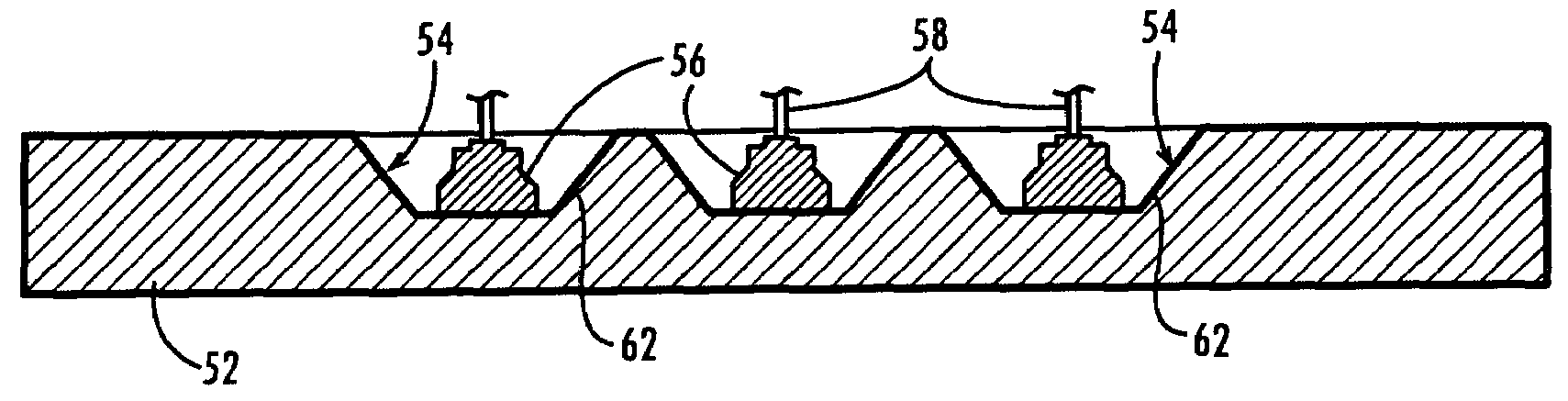
[0038]Representative embodiments of the present invention are shown in FIGS. 5-14, wherein similar features share common reference numerals.

[0039]In a basic embodiment, an LED array employs micro-reflectors. The micro-reflectors, generally, collect and collimate light from the LED array. In doing so, the micro-reflectors enhance the array's optical power. In typical applications, the LED array benefits from such enhanced optical power in that it may be physically located further away from a work surface and yet deliver optical power sufficient to enable proper operation.

[0040]FIG. 5 shows a portion of a dense LED array 50 that may be used for applications requiring high optical power density at the working surface. Such applications may include, for example, curing applications ranging from ink printing to the fabrication of DVDs and lithography. One such LED array is shown and described in U.S. patent application Ser. No. 10 / 984,589, filed Nov. 8, 2004, the entire contents of which...


PUM


Abstract

The present invention provides an optical array module that includes a plurality of semiconductor devices mounted on a thermal substrate formed with a plurality of openings that function as micro-reflectors, wherein each micro-reflector includes a layer of reflective material to reflect light. Such material preferably is conductive so as to provide electrical connection for its associated semiconductor device.

Description

RELATED APPLICATIONS[0001]This application claims priority from U.S. Provisional Application Ser. No. 60 / 554,628, filed Mar. 18, 2004, the contents of which are hereby incorporated by reference as recited in full herein for all purposes.BACKGROUND OF THE INVENTION[0002]This invention relates to high-density light emitting diode (LED) arrays and, more particularly, to an LED array that has improved collection and collimation of light.[0003]High-density UV LED arrays may be used for a variety of applications, including, e.g., curing applications ranging from ink printing to the fabrication of DVDs and lithography. Many such applications require a high optical power density at the working surface. However, such power density tends to be unavailable from a typical LED as such LED alone generally is characterized by light distribution that is undesirably divergent.[0004]For example, FIG. 1 is a graphic illustration showing radiation distribution for two typical LEDs 22, 24 mounted on a s...

Claims


Application Information

Patent Timeline
Patent Type & Authority Patents(United States)
IPC IPC(8): H01L33/00H01L25/075H01L29/18H01L33/20H01L33/46H01L33/60H01L33/64
CPCH01L25/0753H01L33/60H01L33/20H01L33/46H01L33/62H01L33/64H01L2924/10253H01L2924/01322H01L2924/09701H01L2224/48091H01L2924/3025H01L2924/00014H01L2924/00
Inventor OWEN, MARK D.ANDERSON, DUWAYNE R.MCNEIL, THOMAS R.SCHREINER, ALEXANDER F.
Owner SILICON VALLEY BANK
Why Eureka
Try Eureka