Ink jet head circuit board, method of manufacturing the same and ink jet head using the same

a technology of circuit boards and ink jets, applied in semiconductor devices, printing, semiconductor/solid-state device details, etc., can solve the problems of power consumption, degrade reliability, short life span, etc., and achieve the effect of reducing the area of heaters, improving printing resolution, and reducing power consumption

Inactive Publication Date: 2010-01-05
CANON KK
View PDF39 Cites 8 Cited by
  • Summary
  • Abstract
  • Description
  • Claims
  • Application Information

AI Technical Summary

Benefits of technology

[0018]It is therefore a main object of this invention to provide an ink jet head circuit board which can reduce the areas of heaters to achieve an improved printing resolution and a higher image quality while at the same time preventing a degradation of heat efficiency, increasing reliability and reducing power consumption.
[0019]Another object of this invention is to provide a small, highly reliable ink jet head with nozzles formed at high density.
[0033]The basic construction of this invention is characterized by forming a protective layer in two layers and by removing one of the two layers from an area above the heater associated with power consumption of the ink jet head to reduce the effective thickness of the protective layer over the heater, thereby improving the heat efficiency and reducing power consumption. Further, because the resistor layer is deposited over the electrode wire layer, the patterning for removing the first protective layer can be done in a wider range than the gap of the electrode wire in which to form the heater. This allows the areas of the heaters to be reduced for higher printing resolution and higher image quality, without reducing the effective bubble generation area.

Problems solved by technology

Further, because the single protective insulation layer alone may not be able to offer a sufficient protection of the resistor layer, there are cases where a layer of a more mechanically stable metal (e.g., Ta; this layer is generally called an anticavitation layer because of its capability to withstand damages from cavitations) is formed over the protective insulation layer 108 of SiO or SiN (see FIG. 2).
In the construction of the conventional protective layer, however, reducing the power consumption and increasing the reliability of the layer and therefore its longevity are contradictory requirements.
If on the other hand the protective layer is too thin, pin holes may be formed in the protective layer to expose the heater resistor or the protective layer may not be able to fully cover stepped portions of wires.
As a result, ink may infiltrate through these insufficiently covered stepped portions, causing corrosions of wires and heater resistors, which in turn results in degraded reliability and shorter life span.
As a result, the actual bubble generation area further decreases, degrading the heat efficiency.
That is, in a present situation calling for reduced areas of the heaters, if the technique disclosed in Japanese Patent No. 3382424 is adopted as is, there is a problem of further degrading the heat efficiency.

Method used


Image

  • Ink jet head circuit board, method of manufacturing the same and ink jet head using the same
  • Ink jet head circuit board, method of manufacturing the same and ink jet head using the same
  • Ink jet head circuit board, method of manufacturing the same and ink jet head using the same

Examples


second embodiment

of Ink Jet Head Circuit Board

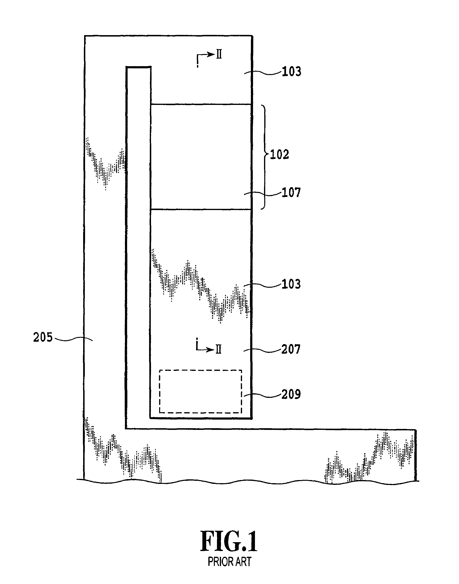
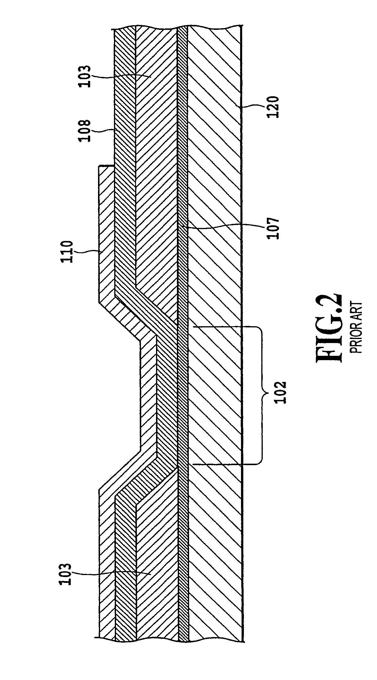
[0075]The first embodiment concerns an ink jet head circuit board in which, as shown in FIG. 6, one heater is provided on the electrode wire for one nozzle. The present invention can also be applied effectively to an ink jet head circuit board in which two or more heaters are provided on the electrode wire for one nozzle.

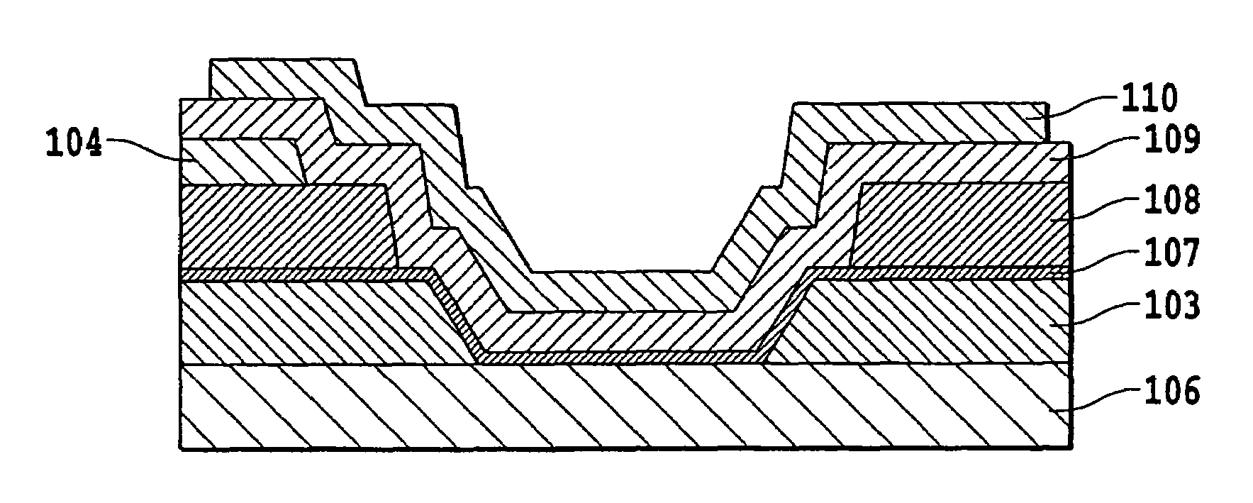
[0076]FIG. 13 shows one such example and is a schematic plan view of a construction in which two heaters 102 are provided in series on an electrode wire 103 for one nozzle. The two heaters are formed simultaneously by the same process as that of the first embodiment, i.e., by forming or patterning the resistor layer over the formed or patterned electrode wire layer 103. Then, the first protective insulation layer 108a is formed over the resistor layer and then removed from an area 301′ to form a pattern shown in FIG. 13.

[0077]This construction has an advantage that since the two heaters combined offer a high resistance, a heat loss by ot...

third embodiment

of Ink Jet Head Circuit Board and Process of Manufacturing the Same

[0079]In the ink jet heads using thermal energy for ink ejection, there are growing demands for increasing the number of nozzles for further miniaturization and higher integration density of circuit board in order to meet the requirements of higher resolution, higher image quality and faster speed. In response to this trend, the number of heaters provided in the circuit board is also increasing and the associated technologies to fabricate the circuit board in small size and at high integration density are being called for. This in turn calls for improved heat efficiency and reduced power consumption. From the standpoint of power saving, it is strongly desired that the resistance of the electrode wires connected to the heater resistors be reduced. The resistance reduction of electrode wire is normally achieved by increasing the width of the electrode wire formed on the substrate. However, as the number of energy gener...


PUM


Abstract

An ink jet head circuit board is provided which has heaters to generate thermal energy for ink ejection as they are energized. This circuit board reduces areas of the heaters to achieve higher printing resolution and image quality. This board also prevents a degradation of thermal energy efficiency and reduces power consumption. The protective insulation layer for the electrode wire layer is formed of two layers and one of the two layers is removed from above the heater to improve the heat energy efficiency. The resistor layer is deposited over the electrode wire layer. The patterning for removing the protective insulation layer is done in a wider range than a gap of the electrode wire layer, the gap being used to form the heater. Further, by forming the electrode wires in two layers, a possible reduction in an effective bubble generation area of the heater can be prevented.

Description

BACKGROUND OF THE INVENTION[0001]1. Field of the Invention[0002]The present invention relates to a circuit board for an ink jet head that ejects ink for printing, a method of manufacturing the circuit board, and an ink jet head using the circuit board.[0003]2. Description of the Related Art[0004]An ink jet printing system has an advantage of low running cost because an ink jet head as a printing means can easily be reduced in size, print a high-resolution image at high speed and even form an image on so-called plain paper that is not given any particular treatment. Other advantages include low noise that is achieved by a non-impact printing system employed by the print head and an ability of the print head to easily perform color printing using multiple color inks.[0005]There are a variety of ejection methods available for the ink jet head to realize the ink jet printing system. Among others, ink jet heads using thermal energy to eject ink, such as those disclosed in U.S. Pat. Nos. ...

Claims


Application Information

Patent Timeline
Patent Type & Authority Patents(United States)
IPC IPC(8): B41J2/05
CPCB41J2/14072B41J2/14129B41J2/1603B41J2/1628B41J2/1646
Inventor SAKAI, TOSHIYASUOZAKI, TERUOONO, KENJISAITO, ICHIROYOKOYAMA, SAKAIIBE, SATOSHISHIBATA, KAZUAKI
Owner CANON KK
Why Eureka
Try Eureka