Sequentially-accessed 1R/1W double-pumped single port SRAM with shared decoder architecture

a single-port, decoder technology, applied in the direction of information storage, static storage, digital storage, etc., can solve the problems of not being able to operate an sram at twice an already aggressive clock frequency, requiring substantial additional power, and using two-port sram circuits

Active Publication Date: 2010-01-05
NVIDIA CORP
View PDF13 Cites 35 Cited by
  • Summary
  • Abstract
  • Description
  • Claims
  • Application Information

AI Technical Summary

Problems solved by technology

Thus, integrated circuits where instances of SRAM circuits are a significant portion of the overall die area, using two-port SRAM circuits can be an extremely expensive design option.
However, this solution involves generating an additional clock reference that is exactly twice the original clock frequency and generally requires substantial additional power.
Furthermore, in high-performance designs, operating an SRAM at twice an already aggressive clock frequency may not be possible.

Method used


Image

  • Sequentially-accessed 1R/1W double-pumped single port SRAM with shared decoder architecture
  • Sequentially-accessed 1R/1W double-pumped single port SRAM with shared decoder architecture
  • Sequentially-accessed 1R/1W double-pumped single port SRAM with shared decoder architecture

Examples


Embodiment Construction

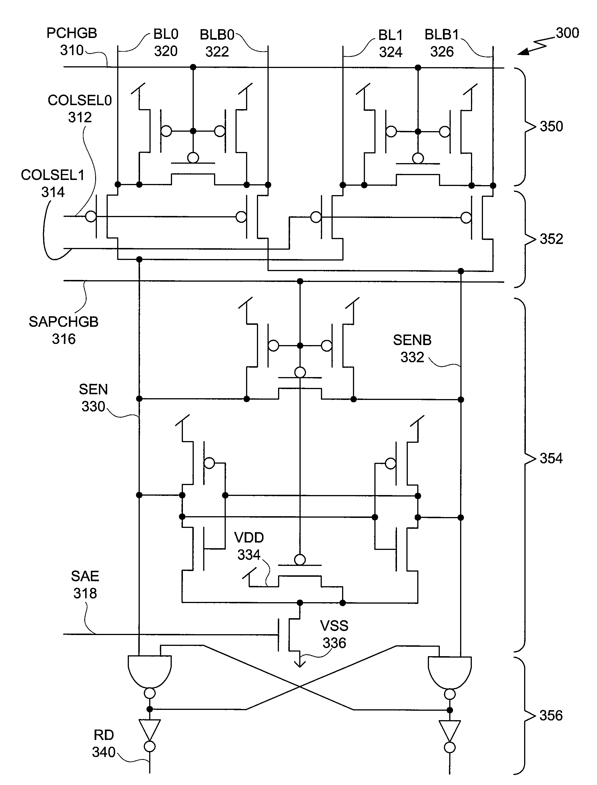
[0018]FIG. 1 illustrates the circuit design of a six-transistor (6T) static random access memory (SRAM) cell 100, according to one embodiment of the invention. The 6T SRAM cell 100 includes two p-channel field effect transistors (P-FETs) 150, 152, four n-channel field effect transistors (N-FETs) 140, 142, 144 and 146. The 6T SRAM cell is connected to a word line (WL) 110, a bit line (BL) 112, and a bit line bar (BLB) 114.

[0019]P-FET 150 and N-FET 144 form a first logic inverter, with output bit 120. P-FET 152 and N-FET 146 form a second logic inverter, with output bitb 122. P-FETs 150 and 152 are connected to a positive supply voltage, conventionally called “VDD”130 in complimentary symmetry metal-oxide semiconductor (CMOS) circuits. N-FETs 144 and 146 are connected to the zero-voltage reference node (or “ground”), conventionally called “VSS”132 in CMOS circuits. The output of the first logic inverter, bit 120, is connected to the input of the second logic inverter, formed by the ga...


PUM


Abstract

One embodiment of the present invention sets forth a synchronous two-port static random access memory (SRAM) design with the area efficiency of a one-port SRAM. By restricting both access ports to an edge-triggered, synchronous clocking regime, the internal timing of the SRAM can be optimized to allow high-performance double-pumped access to the SRAM storage cells. By double-pumping the SRAM storage cells, one read access and one write access are possible per clock cycle, allowing the SRAM to present two external ports, each capable of performing one transaction per clock cycle.

Description

BACKGROUND OF THE INVENTION[0001]1. Field of the Invention[0002]Embodiments of the present invention relate generally to static random access memory (SRAM) design and more specifically to a sequentially-accessed 1R / 1W double-pumped single port SRAM with a shared decoder architecture.[0003]2. Description of the Related Art[0004]Integrated circuits commonly embed SRAM circuits to provide on-chip data storage. A given instance of an SRAM circuit is typically configured to meet specific design requirements associated with the surrounding circuitry attached to the SRAM. One common type of SRAM circuit provides one port for either read or write access to data stored within the SRAM. The address inputs to such a circuit are typically shared for both read and write access. Another common type of SRAM circuit, referred to as a two-port SRAM, provides two ports for accessing data stored within the SRAM. Two-port SRAM circuits usually restrict all read accesses to one port and all write access...

Claims


Application Information

Patent Timeline
Patent Type & Authority Patents(United States)
IPC IPC(8): G11C11/00
CPCG11C11/412G11C11/413
Inventor LIN, HWONG-KWOYANG, GEFRAZIER, ETHAN A.YOUNG, CHARLES CHEW-YUEN
Owner NVIDIA CORP
Why Eureka
Try Eureka