Buffer component for a memory module, and a memory module and a memory system having such buffer component

a buffer component and memory module technology, applied in the field of buffer components for memory modules, can solve the problems of not being able to predict the exact amount of delay time between the presence of address and command signals and the presence of control signals, and the customary procedure of eliminating this problem by providing delay elements is therefore difficult, and the signal cannot be transmitted at the full clock frequency

Active Publication Date: 2010-01-12
POLARIS INNOVATIONS LTD
View PDF12 Cites 3 Cited by
  • Summary
  • Abstract
  • Description
  • Claims
  • Application Information

AI Technical Summary

Benefits of technology

[0009]One embodiment of the present invention provides a buffer component for a memory module in which the problem of the reliable acceptance of the command and address signals into the memory components on account of different signal propagation times on the bus lines is minimized or eliminated.
[0010]Another embodiment of the present invention provides a memory module having a plurality of memory components and a buffer component in which the problem of different signal propagation times on the bus lines of a common signal bus is reduced or eliminated.
[0011]A further embodiment of the present invention provides a memory system having a plurality of memory modules and a memory controller in which a reduction of the access speed to the memory modules on account of reduced access speed is avoided.
[0012]Yet another embodiment of the present invention provides a method for operating a buffer component which minimizes or eliminates the problem of the reliable acceptance of the command and address signals into the memory components on account of different signal propagation times on the signal lines.
[0015]In one embodiment, the control unit may be provided in such a way that, depending on a configuration value provided, it either applies the address and command signals to the plurality of memory components during the first clock period and applies the control signal for activating the group of the plurality of memory components to the group of the plurality of memory components when command and address signals are present in the succeeding second clock period, or applies the address and command signals to the memory components and the control signal to the group of the plurality of memory components to be activated during the same clock period. In this way, a memory module provided with such a buffer component can be configured in a manner dependent on the load on the signal lines, that is to say, e.g., in a manner dependent on the load on account of the quantity of memory components, so that it is possible to provide an operating mode with a low load on the signal lines (e.g., when there is a small quantity of connected memory components) and an operating mode for a large load on the signal lines (e.g., when there is a large quantity of memory components).
[0022]The memory components are provided so as to receive or transmit data signals in a burst mode, the length of the burst in which the data signals are transmitted in accordance with an activation by the corresponding control signal depending on the configuration value provided in the buffer component. In this way, it is possible to vary the length of the burst mode depending on the operating mode of the memory module, so that, in the case of an activation during a second clock period following a first clock period, the burst length is increased in order to be able to ensure the volume of data to be transmitted even in the case of operation of the memory module with a reduced data rate during which the control signals are not applied until during the second clock period.

Problems solved by technology

The customary procedure for eliminating this problem by providing delay elements is therefore difficult because the different propagation times of the signals on the bus lines for the address and command signals and for the control signals are not known from the outset if the number of memory components used on a memory module is variable.
As a result, the amount of the delay time between the presence of the control signals and the presence of the address and command signals cannot be predicted exactly.
Particularly in the case of memory modules having a plurality of groups of memory components, due to the high load on the bus lines for the address and command signals, these signals can no longer be transmitted at the full clock frequency since the signals are subjected to considerable interference on the path from the buffer component to the corresponding memory component.

Method used


Image

  • Buffer component for a memory module, and a memory module and a memory system having such buffer component
  • Buffer component for a memory module, and a memory module and a memory system having such buffer component
  • Buffer component for a memory module, and a memory module and a memory system having such buffer component

Examples


Embodiment Construction

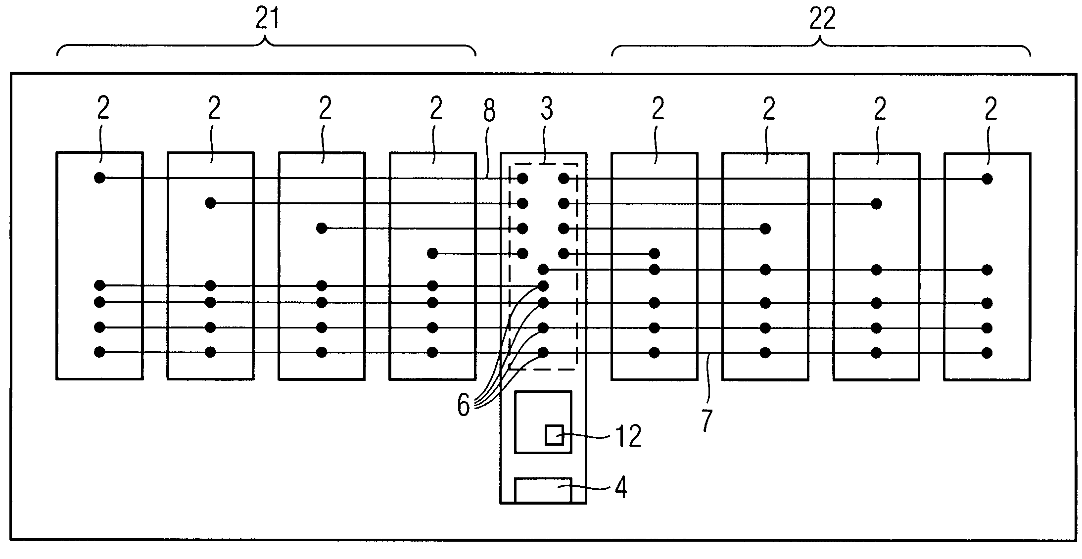
[0031]FIG. 1 illustrates a block diagram of a memory module 1 according to one embodiment of the invention. The memory module 1 comprises eight memory components 2 connected to a buffer component 3. The memory module 1 is formed, for example, in the form of a printed circuit board on which are situated signal lines 7 to which the memory components 2 and the buffer component 3 are connected.

[0032]The buffer component 3 has a data transmission interface 4, via which the memory module 1 receives, from externally, an item of access information in order to write data, read out data or perform other functions in the memory components 2. The access information is provided to a control unit 5 for the buffer component 3, in which the access information is divided and / or converted into suitable address, clock, control and command signals for driving the memory components 2.

[0033]In the present exemplary embodiment, the memory components 2 are preferably DRAM memory components, but may also be...


PUM


Abstract

A buffer component for a memory module having a plurality of memory components includes item of access information in accordance with a data transmission protocol, the address, clock, control and command signals depending on the access information, a second data interface for driving a clock signal and address and command signals to the plurality of memory components and for driving a control signal to a group of the plurality of memory components in accordance with a signaling protocol, wherein an activation of the memory components and an acceptance of the address and command signals are effected in a manner dependent on the control signals, and a control unit which applies the address and command signals to the plurality of memory components during a first clock period of the clock signal and applies the control signal for activating the group of the plurality of memory components to the group of the plurality of memory components to be activated when address and command signals are present, in a succeeding second clock period of the clock signal, whereby the address and command signals present are accepted into the group of the plurality of memory components.

Description

CROSS-REFERENCE TO RELATED APPLICATIONS[0001]This application claims foreign priority benefits under 35 U.S.C. §119 to co-pending German patent application number DE 10 2005 009 806.1, filed 3 Mar. 2005. This related patent application is herein incorporated by reference in its entirety.BACKGROUND OF THE INVENTION[0002]1. Field of the Invention[0003]The invention relates to a buffer component for a memory module having a plurality of memory components. The invention further relates to a memory module having a plurality of memory components and a buffer component. Furthermore, the invention relates to a memory system having at least two memory modules and a memory controller that provides items of access information for the memory modules.[0004]2. Description of the Related Art[0005]In new types of memory modules, so-called “fully buffered dual in-line memory modules (DIMMs)”, the memory components situated thereon are for example no longer directly connected to the memory controller...

Claims


Application Information

Patent Timeline
Patent Type & Authority Patents(United States)
IPC IPC(8): G11C7/10
CPCG06F13/1689G11C5/04G11C5/063G11C7/1078G11C7/109
Inventor BRAUN, GEORGDJORDJEVIC, SRDJANJAKOBS, ANDREAS
Owner POLARIS INNOVATIONS LTD
Why Eureka
Try Eureka