Metal electrical fuse structure

a metal electrical fuse and fuse body technology, applied in the field of semiconductor structures, can solve the problems of laser fuses not being scaled proportionally with other devices, structure may suffer reliability problems, and suffer scalability problems, etc., to achieve high scalability, improve reliability, and stop cracking

Inactive Publication Date: 2010-01-26
TAIWAN SEMICON MFG CO LTD
View PDF9 Cites 28 Cited by
  • Summary
  • Abstract
  • Description
  • Claims
  • Application Information

AI Technical Summary

Benefits of technology

[0012]In accordance with another aspect of the present invention, a method for forming the preferred embodiments of the present invention includes forming a shallow trench isolation region, forming a first dielectric layer over the shallow trench isolation region, forming a contact plug extending from a top surface of the first dielectric layer to the shallow trench isolation region wherein the contact plug comprises a middle portion being substantially narrower than two end portions, forming a second dielectric layer over the first dielectric layer, and forming two metal lines in the second dielectric layer wherein each of the two metal lines is connected to different ones of the end portions of the contact plug. The method further includes forming a polysilicon strip to narrow the narrow portion of the contact plug. A guard line may be formed on each side of the contact plug to stop cracking caused by heat.
[0013]The advantageous features of the preferred embodiments of the present invention include improved reliability, high scalability and full compatibility with the existing integrated circuit formation processes.

Problems solved by technology

However, they suffer scalability problems.
A certain size is desired for accurate blowing, thus the laser fuses cannot be scaled proportionately with other devices.
This structure may suffer reliability problems, since the resistivity of polysilicon line 2 is determined by the doping concentration, and may vary from process to process.
This embodiment suffers scalability problems.
A possible problem for the structure is that after the contact 19 is blown by heat and an open circuit forms, remaining heat may cause silicidation of tungsten with polysilicon plate 12, and a low resistivity path of silicide reconnects the disconnected parts.

Method used


Image

  • Metal electrical fuse structure
  • Metal electrical fuse structure
  • Metal electrical fuse structure

Examples


Embodiment Construction

[0019]The making and using of the presently preferred embodiments are discussed in detail below. It should be appreciated, however, that the present invention provides many applicable inventive concepts that can be embodied in a wide variety of specific contexts. The specific embodiments discussed are merely illustrative of specific ways to make and use the invention, and do not limit the scope of the invention.

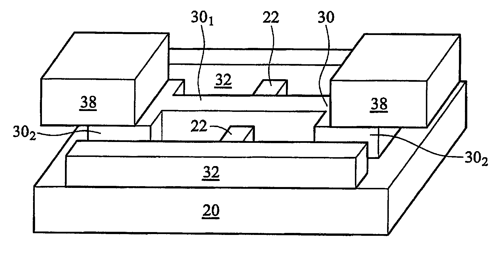
[0020]The cross-sectional views, perspective views and top views of the intermediate stages in the manufacturing of the preferred embodiments of the present invention are illustrated in FIGS. 3 through 11. Throughout the various views and illustrative embodiments of the present invention, like reference numbers are used to designate like elements. Each figure number may be followed by a letter A or B, which letters indicate different variations or views.

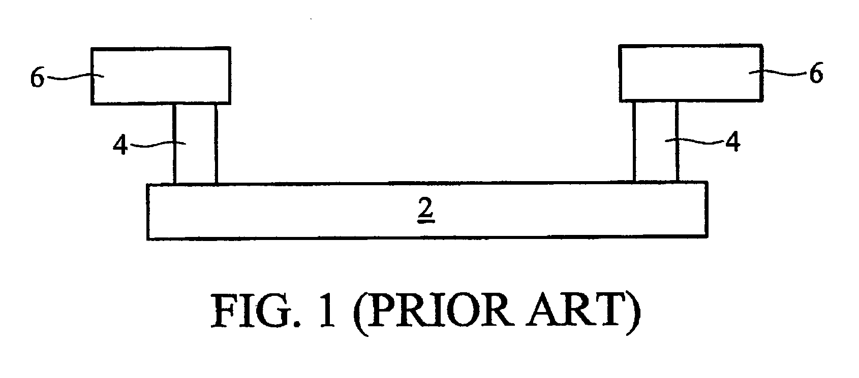
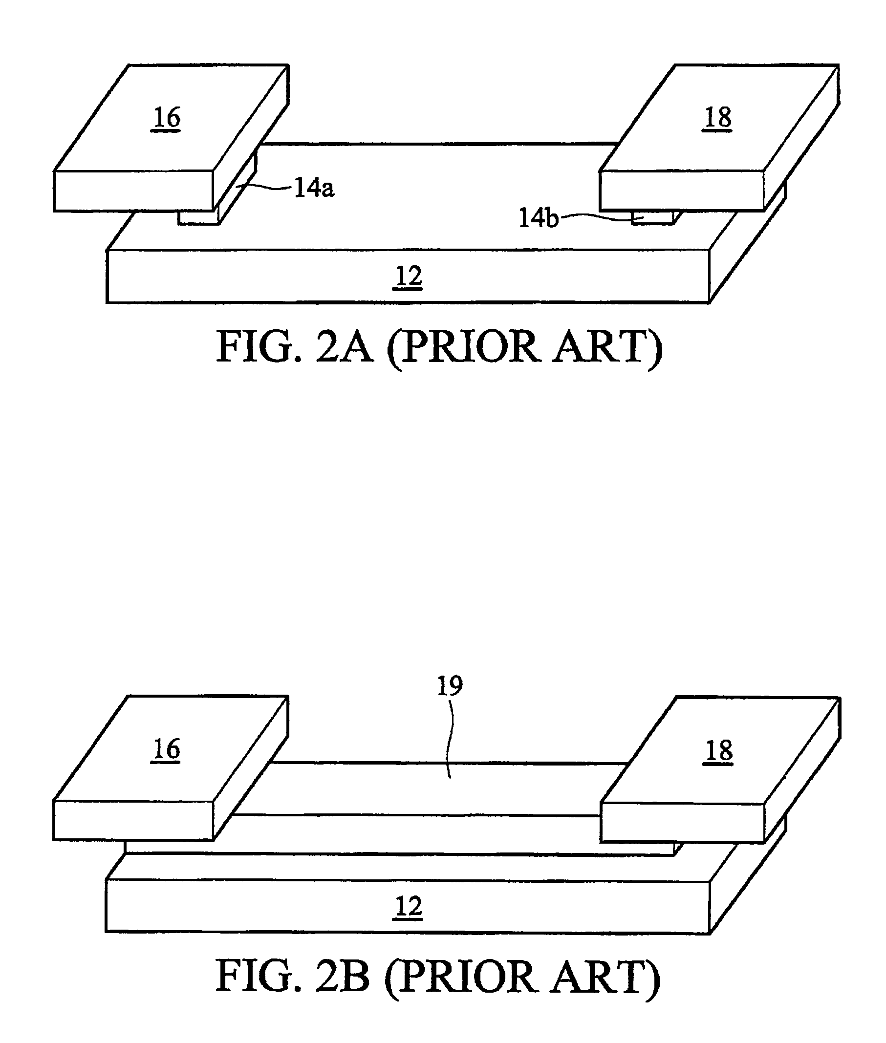
[0021]FIGS. 3A, 3B and 3C illustrate the formation of a polysilicon strip 22 on a dielectric isolation region 20, which is f...


PUM


Abstract

An electrical fuse and a method for forming the same are provided. The electrical fuse includes a dielectric layer over a shallow trench isolation region and a contact plug extending from a top surface of the dielectric layer to the shallow trench isolation region, wherein the contact plug comprises a middle portion substantially narrower than the two end portions. The contact plug forms a fuse element. The electrical fuse further includes two metal lines in a metallization layer on the dielectric layer, wherein each of the two metal lines is connected to different ones of the end portions of the contact plug.

Description

TECHNICAL FIELD[0001]This invention relates generally to semiconductor structures, and more particularly to electrical fuses and a fabrication method thereof.BACKGROUND[0002]In the semiconductor industry, fuse elements are widely used in integrated circuits for a variety of purposes, such as improving manufacturing yield or customizing a generic integrated circuit. For example, by replacing defective circuits on a chip with duplicate or redundant circuits on the same chip, manufacturing yields can be significantly increased. A fuse disconnected by a laser beam is referred to as a laser fuse, while a fuse disconnected by passing an electrical current, or blowing, is referred to as an electrical fuse, or e-fuse. By selectively blowing fuses within an integrated circuit, which has multiple potential uses, a generic integrated circuit design may be economically manufactured and adapted to a variety of customer uses.[0003]Typically, fuses are incorporated in the design of the integrated ...

Claims


Application Information

Patent Timeline
Patent Type & Authority Patents(United States)
IPC IPC(8): H01L21/82
CPCH01L23/5256H01L2924/3011H01L2924/0002H01L2924/00
Inventor CHEN, HSUEH-CHUNGTSAI, HAO-YICHEN, HSIEN-WEIJENG, SHIN-PUUHOU, SHANG-YUN
Owner TAIWAN SEMICON MFG CO LTD
Why Eureka
Try Eureka