

Method for forming silazane-based dielectric film
a dielectric film and silazane technology, applied in the field of silazane-containing dielectric films, can solve the problems of insufficient filling performance, significant shrinkage of films, and film breakag
- Summary
- Abstract
- Description
- Claims
- Application Information
AI Technical Summary
Benefits of technology
Problems solved by technology
Method used
Image

Examples
example 1
Evaluation Results of SiNCH Silazane Process
[0076]Films were formed under the conditions shown in Table 1 and below, and the film characteristics were examined an hour after the heat treatment at 900° C.
[0077]Process Sequence:
[0078]Film forming: Temperature 0° C., pressure 266.6 Pa
[0079]H2O annealing: 1 hour of steam processing at 130° C. (H2O flow rate 1 g / min)
[0080]Heat treatment: 1 hour of O2 / N2 processing at 400° C. (N2 1 SLM, pressure 800 Pa; the experiment was conducted using a chamber separate from the one used for H2O processing.)
[0081]High-temperature heat treatment: 1 hour of N2 processing at 900° C. (N2 flow rate 1 SLM, atmospheric pressure)
[0082]As shown in Table 1, silazane-based films formed without using organic solvent, but using a material containing carbon and an additive gas not containing carbon, exhibited improved filling characteristics through lowering of the RF power when the electrode gap was narrow. When the electrode gap was wide, no problem occurred even ...
example 2
Evaluation Results of SiNH Silazane Process
[0084]Films were formed under the conditions shown in Table 2 and below, and the film characteristics were examined an hour after the heat treatment at 900° C.
[0085]Process Sequence:
[0086]Film forming: Temperature 0° C., pressure 266.6 Pa
[0087]H2O annealing: 1 hour of steam processing at 130° C. (H2O flow rate 1 g / min)
[0088]Heat treatment: 1 hour of O2 / N2 processing at 400° C. (N2 1 SLM, pressure 800 Pa; the experiment was conducted using a chamber separate from the one used for H2O processing.)
[0089]High-temperature heat treatment: 1 hour of N2 processing at 900° C. (N2 flow rate 1 SLM, atmospheric pressure)
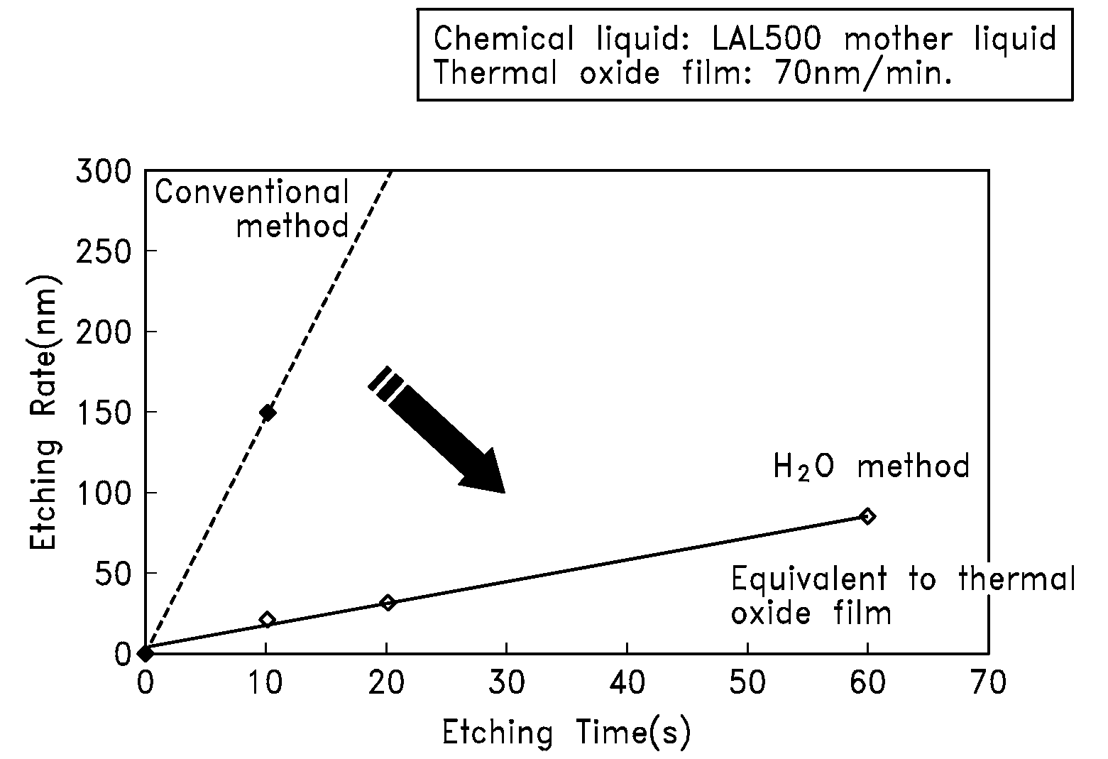
[0090]Chemical-solution resistance evaluation: A stock solution of LAL500 was used to conduct the evaluation. A thermal oxide film was used as a reference. The etch rate of the thermal oxide film was 43 nm / min. The decrease in film thickness at the top of the STI structure was calculated based on the cross-section observation result.
[00...
example 3
Dependence of Film Characteristics by Heat Treatment Sequence
[0093]Films were formed under the conditions shown in Table 3 and below, and the film characteristics were examined. The initial surface hardening sequence represents a sequence without H2O annealing, while the initial liquid processing sequence represents one with H2O annealing.
[0094]Film Forming Conditions:
[0095]Susceptor temperature: 0° C.
[0096]Material flow rate: 1,1,3,3-TMDS 30 sccm
[0097]Additive gas flow rate: NH3 20 sccm
[0098]He flow rate: 2 SLM
[0099]Pressure: 266 Pa
[0100]13.56-MHz power: 28 W
[0101]Discharge gap: 400 mm
[0102]The normal logic is that as the film shrinkage increases, the film density increases when the volume of film starts to shrink. As shown in Table 3, however, the film density resulting after H2O annealing was higher than when H2O annealing was not performed, despite the very low film shrinkage rate. A possible cause is the difference in the carbon dissociation and the Si—O replacement steps under...
PUM
| Property | Measurement | Unit |
|---|---|---|
| temperature | aaaaa | aaaaa |
| temperature | aaaaa | aaaaa |
| temperature | aaaaa | aaaaa |
Abstract
Description
Claims
Application Information