
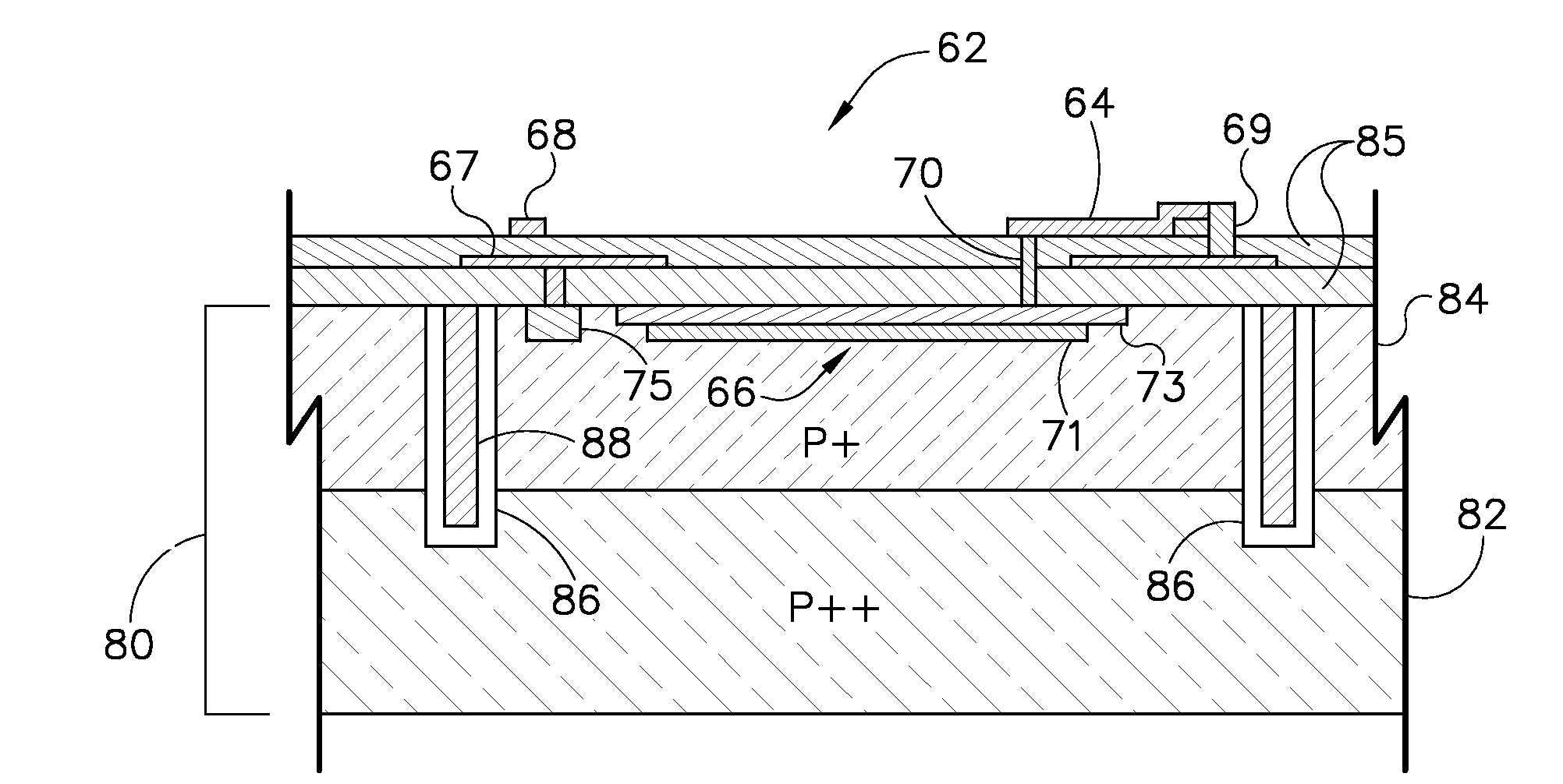
Structure of a solid state photomultiplier

a photomultiplier and solid-state technology, applied in the field of imaging radiometers, can solve the problems of inability to provide data or feedback as to the number and/or energy of photons detected, inability to provide energy discriminatory data or otherwise count the number and/or energy of photons actually received by a given detector element or pixel, and inability of photodiodes to discriminate between the energy levels. , to achieve the effect of improving the optical crosstalk and dark count ra

Active Publication Date: 2010-01-26
GENERAL ELECTRIC CO
View PDF4 Cites 16 Cited by
  • Summary
  • Abstract
  • Description
  • Claims
  • Application Information

AI Technical Summary

Benefits of technology

"The present invention provides a solid-state photomultiplier with improved optical crosstalk and dark count rate characteristics. The optical isolation structure containing a light absorbing material or a light reflecting material deposited therein separates each avalanche photodiode cell from adjacent cells. The method of manufacturing the solid-state photomultiplier includes the steps of forming a semiconductor substrate, placing an epitaxial layer on the substrate, and positioning a plurality of avalanche photodiodes on the epitaxial layer. The detector module includes a scintillator and a solid-state photomultiplier coupled to the scintillator, which converts the optical photons into corresponding electrical signals. The isolation trench grid includes at least one of a light absorbing material and a light reflecting material therein."

Problems solved by technology

A drawback of such detectors however is their inability to provide data or feedback as to the number and / or energy of photons detected.
These detectors, however, are unable to provide energy discriminatory data or otherwise count the number and / or measure the energy of photons actually received by a given detector element or pixel.
Under the charge integration operation mode, the photodiode is not capable of discriminating between the energy level or the count of X-rays received by the scintillator.
The benefits set forth above make the use of an SSPM in a detector desirable for numerous reasons; however, there are varying problems that affect current SSPM designs.
When the emitted light is absorbed, it can trigger additional avalanche events, which also cause light emission.
The final result can be a large number of APDs avalanching for a single photon incident on the device, thus resulting in optical crosstalk.
Such a mechanism for controlling optical crosstalk is only somewhat effective, and additionally, results in a loss of active area in the SSPM.
That is, the spacing between adjacent APDs limits the fill factor of the active area of the SSPM and makes it difficult to design APD cell size smaller than approximately 30 microns without substantial active area loss.
Another issue with current SSPM designs is the potentially high dark count rate resulting from the whole bulk of the silicon wafer substrate.
That is, a single layer silicon wafer substrate design in an SSPM can result in high diffusion dark leakage, thus adding to the overall dark count rate.

Method used


Image

  • Structure of a solid state photomultiplier
  • Structure of a solid state photomultiplier
  • Structure of a solid state photomultiplier

Examples


Embodiment Construction

[0024]The present invention is directed to radiographic detectors for imaging and, more particularly, to a solid-state photomultiplier (SSPM) structure with improved crosstalk and dark count rate characteristics. The SSPM can be integrated into any number of radiographic detection devices, including gamma spectrometers / isotope identifiers, neutron detectors, computed tomography systems, and positron emission tomography (PET) systems.

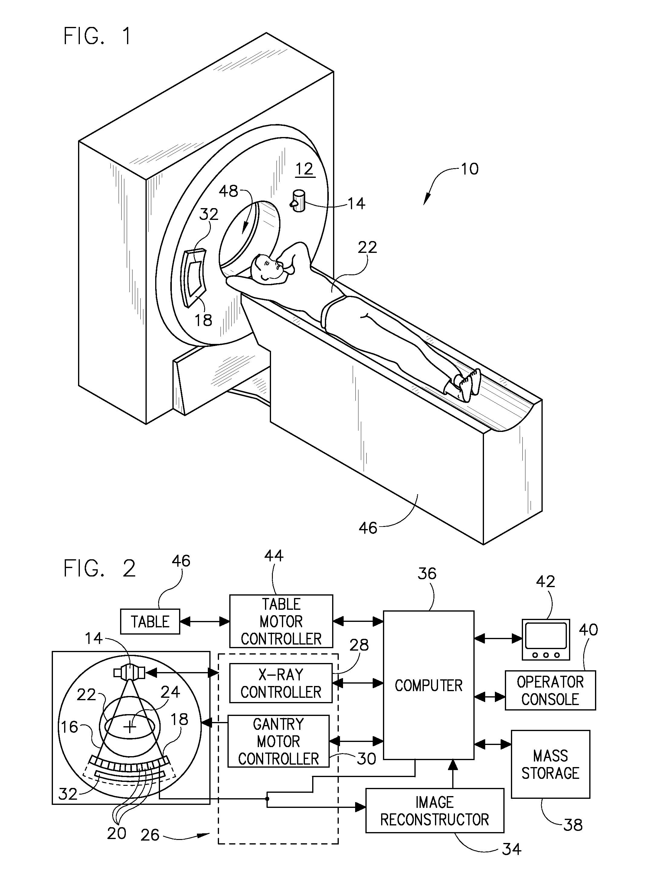
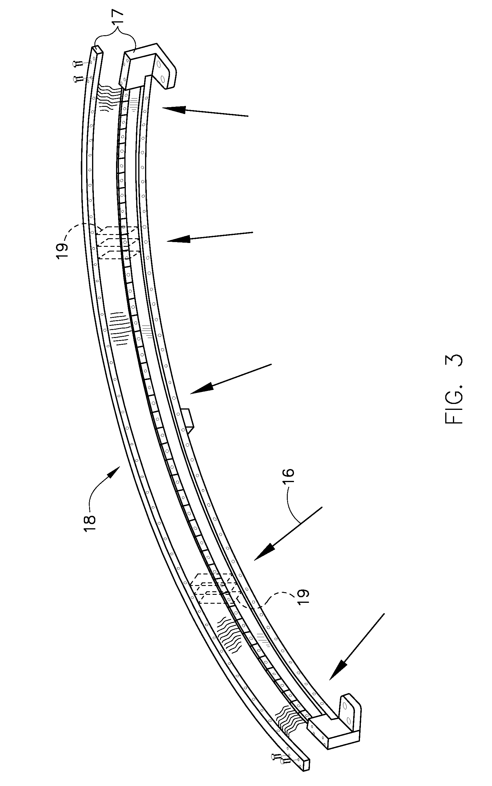
[0025]In accordance with one aspect of the present invention, a CT imaging system is provided. The CT imaging system includes a detector constructed to perform photon counting and energy discrimination of x-rays at the high flux rates generally associated with CT imaging. Referring to FIGS. 1 and 2, a computed tomography (CT) imaging system 10 is shown as including a gantry 12 representative of a “third generation” CT scanner. Gantry 12 has an x-ray source 14 that projects a beam of x-rays 16 toward a detector assembly 15 on the opposite side of the gant...


PUM


Abstract

A solid-state photomultiplier (SSPM) includes an optical isolation structure therein. The SSPM includes a substrate and an epitaxial diode layer positioned on the substrate. A plurality of avalanche photodiodes (APDs) are fabricated on the epitaxial diode layer and the optical isolation structure is positioned about the plurality of APDs to separate each of the plurality of APDs from adjacent APDs. The optical isolation structure contains at least one of a light absorbing material and a light reflecting material deposited therein to reduce optical crosstalk and dark count rate in the SSPM.

Description

BACKGROUND OF THE INVENTION[0001]The present invention relates generally to radiographic detectors for imaging and, more particularly, to a solid-state photomultiplier (SSPM) structure with improved crosstalk and dark count rate characteristics.[0002]Typically, in radiographic imaging systems, such as x-ray and computed tomography (CT), an x-ray source emits x-rays toward a subject or object, such as a patient or a piece of luggage. Hereinafter, the terms “subject” and “object” may be interchangeably used to describe anything capable of being imaged. The x-ray beam, after being attenuated by the subject, impinges upon an array of radiation detectors. The intensity of the attenuated radiation received at the detector array is typically dependent upon the attenuation of the x-rays. Each detector element of the detector array produces a separate electrical signal indicative of the attenuated beam received by each detector element. The electrical signals are transmitted to a data proces...

Claims


Application Information

Patent Timeline
Patent Type & Authority Patents(United States)
IPC IPC(8): G01T1/24
CPCG01T1/2018H01L31/107H01L27/14663H01L27/1463G01T1/20182G01T1/20184
Inventor LI, WENZELAKIEWICZ, SCOTT STEPHEN
Owner GENERAL ELECTRIC CO
Learn More