

Probe member for wafer inspection, probe card for wafer inspection and wafer inspection equipment
a technology for wafer inspection and probe cards, which is applied in the direction of measurement devices, semiconductor/solid-state device testing/measurement, instruments, etc., can solve the problems of large inspection cost, long time-consuming and labor-intensive individual electrical inspection, and inability to accurately measure the performance of the probe card, etc., and achieve the effect of stable retention
- Summary
- Abstract
- Description
- Claims
- Application Information
AI Technical Summary
Benefits of technology
Problems solved by technology
Method used
Image

Examples
example 1
[Production of Sheet-Like Probe]
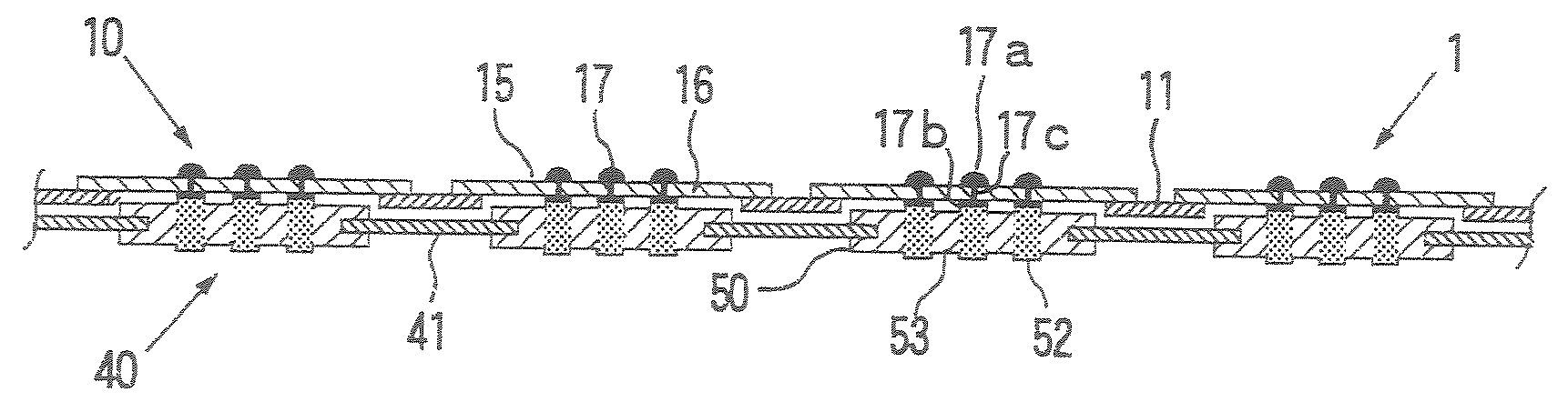
[0311]A frame plate (11) of the following specification was produced in accordance with the construction shown in FIG. 6.
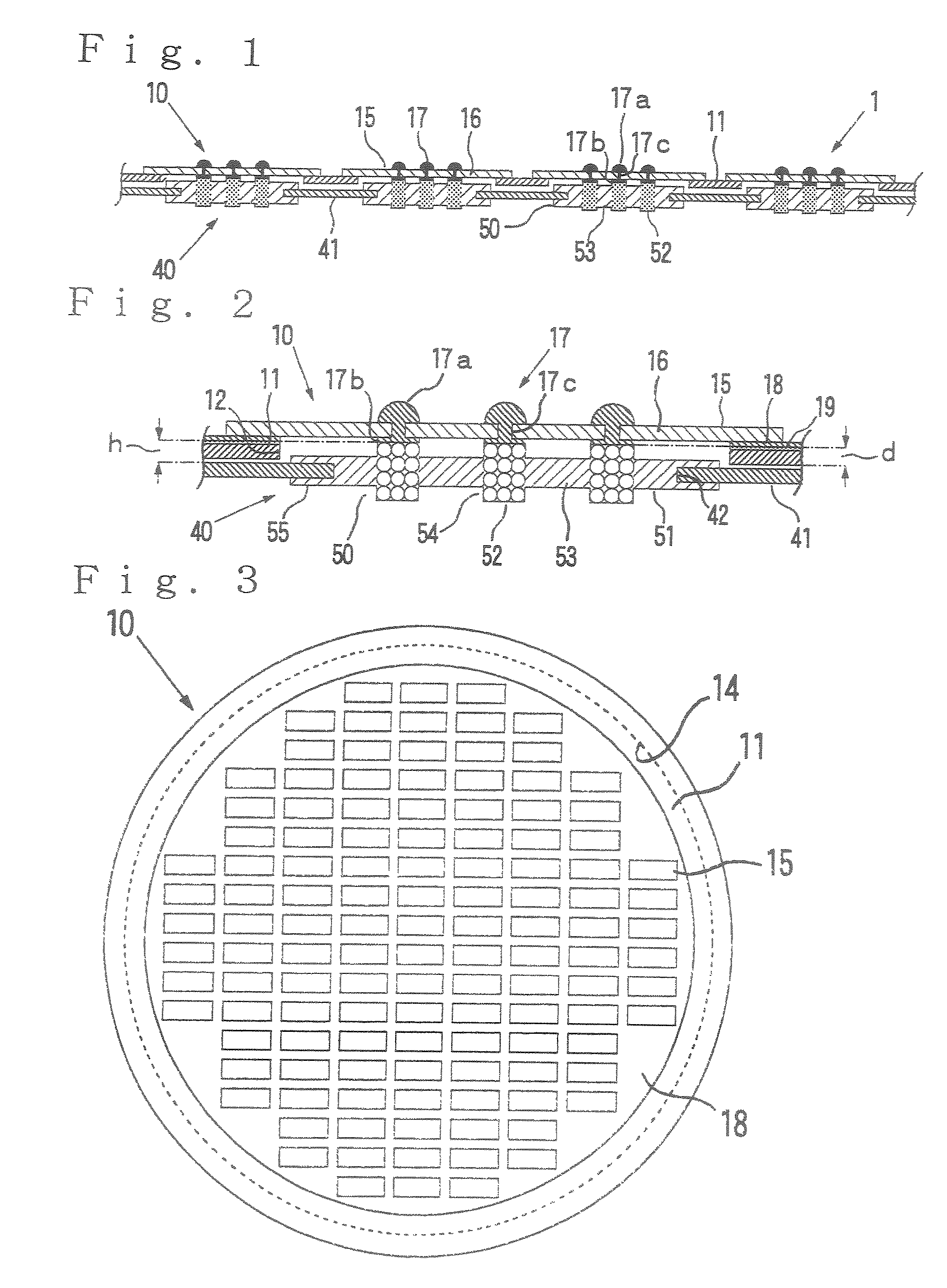
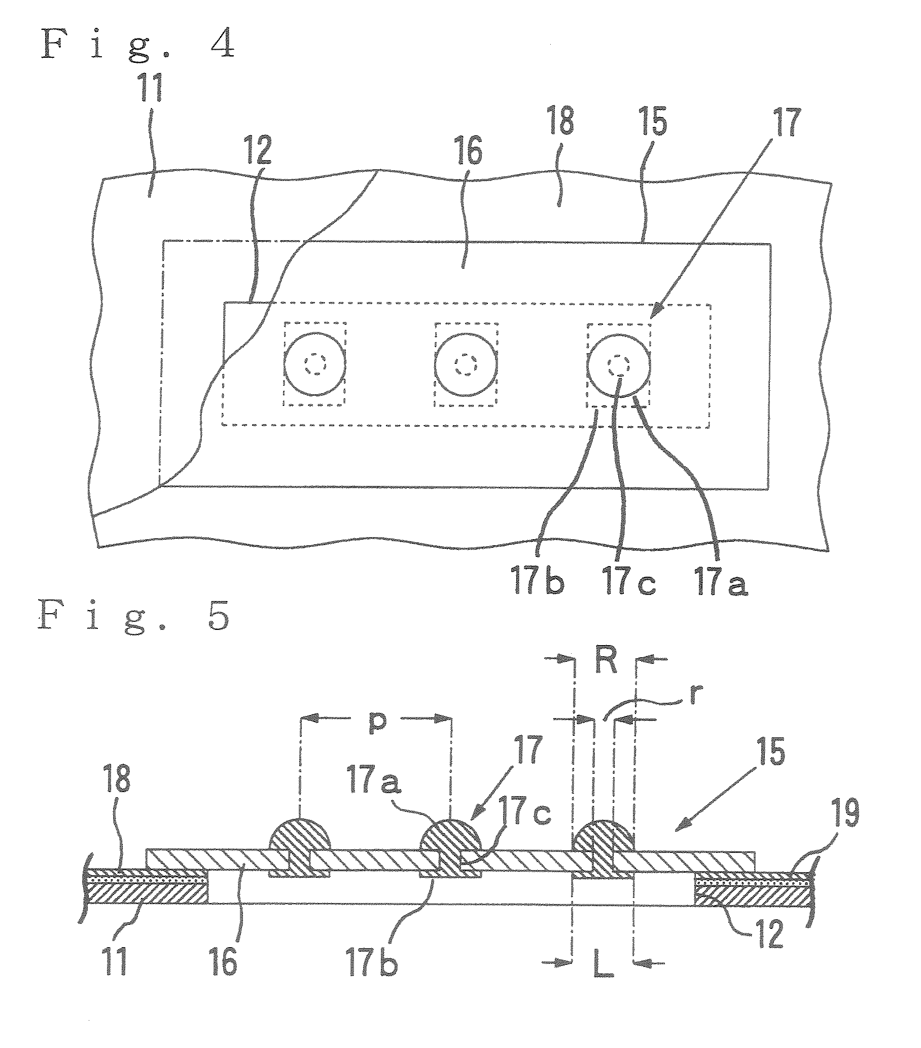
[0312]This frame plate (11) has a circular form having a diameter of 22 cm and a thickness of 25 μm, and 393 openings (12) corresponding to the regions of the electrodes to be inspected of the integrated circuits in Wafer W1 for test. Each of the openings (12) has dimensions of 6.4 mm×1.6 mm.
[0313]A laminate material (21B) obtained by integrally laminating a metal foil (22) for plating electrode and a metal foil (23) for forming holding parts, which each had a diameter of 20 cm and a thickness of 4 μm and were composed of copper, on both surfaces of a resin sheet (21A) for insulating protecting layers, which had a diameter of 20 cm and a thickness of 25 μm and was composed of polyimide, is provided (see FIG. 34).
[0314]A protecting film is formed on the whole front surface of the metal foil (22) for plating electrode by a protecting ...
referential example 1
[0388]A sheet-like probe, an anisotropically conductive connector and a circuit board for inspection were produced in the same manner as in Example 1 except that a frame plate, the thickness of which was 50 μm, was used as the frame plate in the sheet-like probe, and Test 1 and Test 2 were performed. In Referential Example 1, a gap d between the level of the back surface of the frame plate in the sheet-like probe and the level of the electrode surface of the back-surface electrode part is 40 μm, a gap h between the level of the front surface of the frame plate in the anisotropically conductive connector and the level of the front surface-side end surface of the conductive part for connection in the elastic anisotropically conductive film is 35 μm, and a ratio h / d is 0.88.
referential example 2
[0389]A sheet-like probe, an anisotropically conductive connector and a circuit board for inspection were produced in the same manner as in Example 1 except that a frame plate, the thickness of which was 100 μm, was used as the frame plate in the sheet-like probe, and Test 1 and Test 2 were performed. In Referential Example 2, a gap d between the level of the back surface of the frame plate in the sheet-like probe and the level of the electrode surface of the back-surface electrode part is 90 μm, a gap h between the level of the front surface of the frame plate in the anisotropically conductive connector and the level of the front surface-side end surface of the conductive part for connection in the elastic anisotropically conductive film is 35 μm, and a ratio h / d is 0.4.
[0390]The results of the above-described tests are shown in Table 1 and Table 2.
[0391]
TABLE 1Proportion ofInsulation FailureExample 10%Comparative0%Example 1Referencial0%Example 1Referencial0%Example 2
[0392]
TABLE 2C...
PUM
 Abstract
Description
Claims
Application Information