Semiconductor integrated circuit device

a technology of integrated circuit device and semiconductor, which is applied in the direction of pulse technique, pulse generator details, instruments, etc., can solve the problems of increasing power consumption of no optimization of threshold voltage in this semiconductor integrated circuit device, and reducing the effect of process variation and change in operating environment, reducing the adverse effects of process variations and changes, and minimizing the operation power

Active Publication Date: 2010-02-09
NEC CORP
View PDF16 Cites 27 Cited by
  • Summary
  • Abstract
  • Description
  • Claims
  • Application Information

AI Technical Summary

Benefits of technology

[0006]For reducing the power consumption of a semiconductor integrated circuit device, it is important not only to control a power supply voltage, but also to control a threshold voltage. In the semiconductor integrated circuit device disclosed in JP-A-2001-345693, the power supply voltage and the substrate bias voltage are controlled, and the substrate bias voltage is controlled to change the threshold voltage. However, the disclosed semiconductor integrated circuit device is problematic in that since the association table is employed, data relative to a combination of power supply voltages and substrate bias voltages are required in advance. The power supply voltage and the substrate bias voltage for minimizing the power consumption of the semiconductor integrated circuit device differ from semiconductor integrated circuit device to semiconductor integrated circuit device due to various factors involved in the fabrication process for semiconductor integrated circuit devices. Therefore, the data of the association table need to be determined based on actually measured values. Preparing a large amount of association table data greatly complicates the fabrication process for semiconductor integrated circuit devices, and increases the manufacturing cost of the semiconductor integrated circuit devices.
[0007]It is an object of the present invention to provide a semiconductor integrated circuit device which is capable of optimizing a power supply voltage and a threshold voltage for minimizing an operational power with respect to a given operation clock frequency either without an association table or with a small number of association table data.
[0010]In the semiconductor integrated circuit device, it is possible to minimize the operating power by controlling the threshold voltage to make the ratio of the switching current and the leakage current constant at a given clock frequency.
[0012]In the semiconductor integrated circuit device, the threshold voltage is controlled to make the ratio of the switching current and the leakage current constant at a given clock frequency, and the power supply voltage is controlled to guarantee the operating speed, thus making it possible to minimize the operating power while guaranteeing the operating speed.
[0016]According to the present invention, the threshold voltage is dynamically controlled to keep the ratio of the leakage current and the switching current constant, thereby making it possible to achieve a ratio for minimizing the operational power at all times depending on changes in operational environments including the temperature, the power supply voltage, the operating frequency, etc. According to the present invention, therefore, there is provided a semiconductor integrated circuit device which is capable of minimizing the operational power by keeping the ratio of the leakage current and the switching current constant.
[0017]As a result of dynamically controlling the threshold voltage as described above, it is possible to reduce adverse effects of process variations and changes in operational environments including the temperature, the power supply voltage, etc. According to the present invention, therefore, there is provided a semiconductor integrated circuit device which is capable of reducing effects of variations caused by the fabrication process, the temperature, the power supply voltage, etc. by keeping the ratio of the leakage current and the switching current constant.

Problems solved by technology

The semiconductor integrated circuit device has such a tendency that its power consumption increases as the number of transistors which makes up the semiconductor integrated circuit increases.
Therefore, there is no optimization of the threshold voltage in this semiconductor integrated circuit device.
With semiconductor devices being progressively scaled, the proportion of a leakage power in the total power consumption of a semiconductor device is growing.
The results accomplished by K. Nose et al. are based on a theoretical analysis, and they have not clearly specified how to realize such a semiconductor integrated circuit device.

Method used


Image

  • Semiconductor integrated circuit device
  • Semiconductor integrated circuit device
  • Semiconductor integrated circuit device

Examples


Embodiment Construction

[0113]Preferred exemplary embodiments of the present invention will be described in detail below with reference to the drawings.

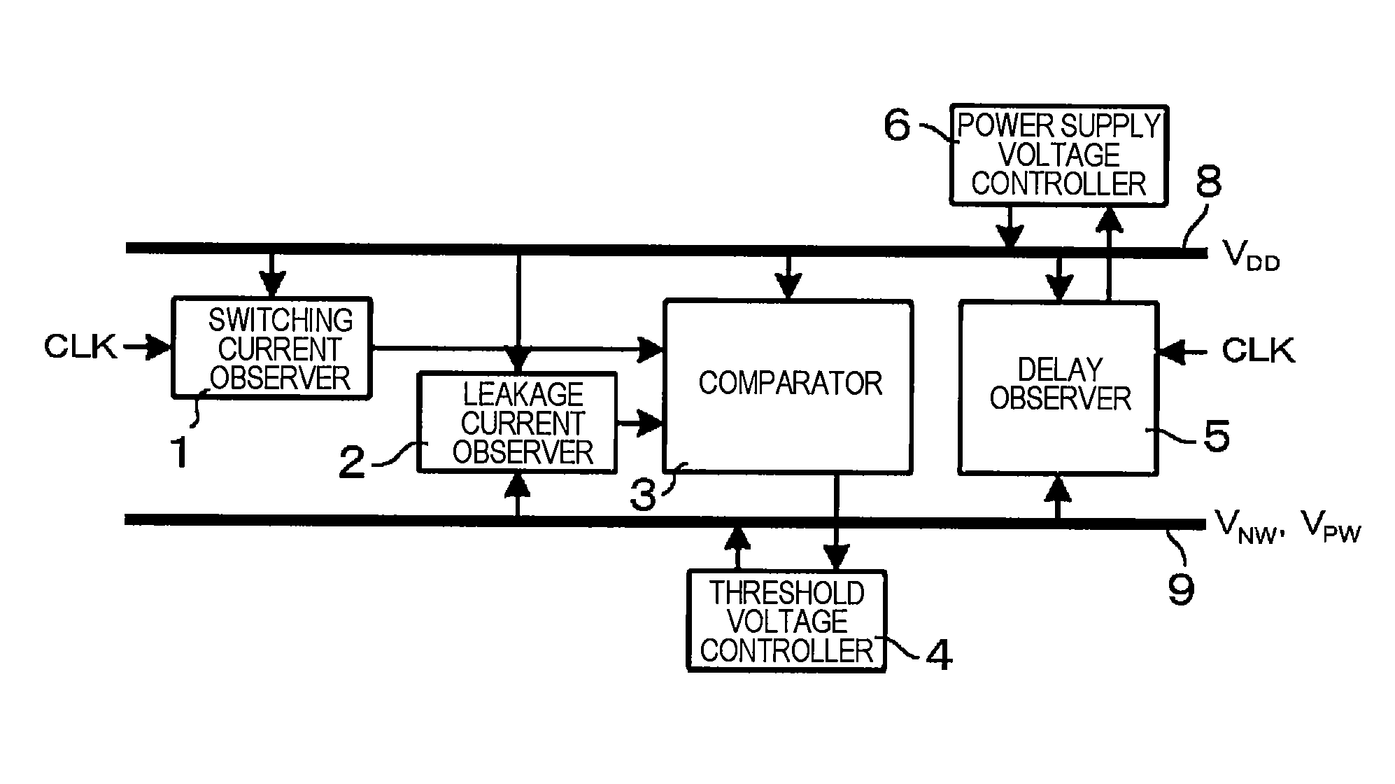
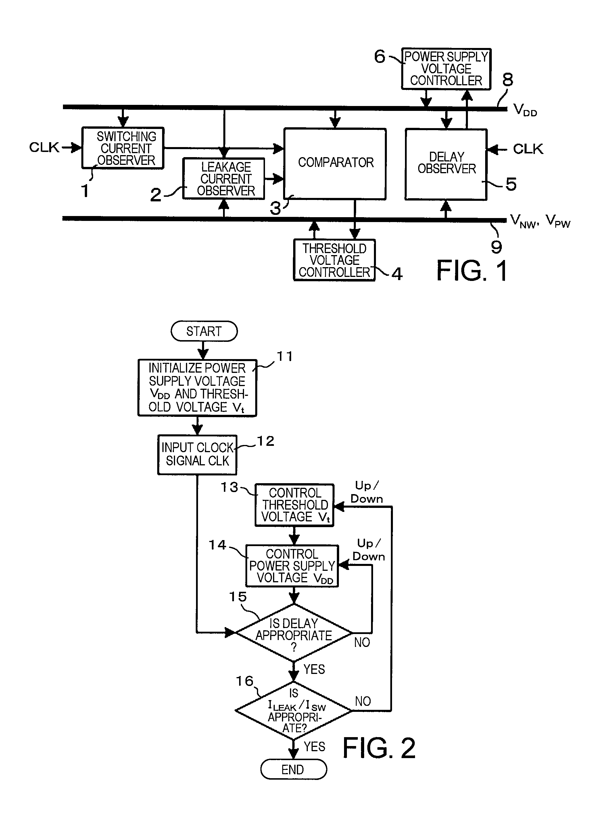
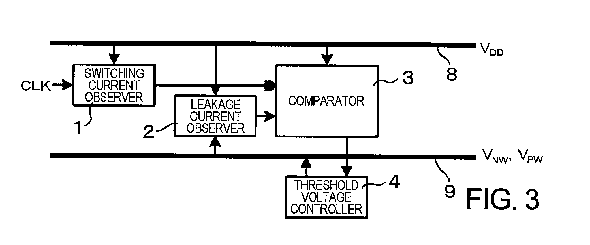
[0114]FIG. 1 shows an overall arrangement of a semiconductor integrated circuit device according to a first exemplary embodiment of the present invention. The semiconductor integrated circuit device includes power supply line 8 for being supplied with power supply voltage VDD and substrate bias line 9 for supplying substrate bias potentials VPW, VNW into a semiconductor integrated circuit. Though not shown, the semiconductor integrated circuit device includes a circuit function part for realizing functions to be originally performed by the semiconductor integrated circuit device, as a CMOS logic circuit. Power supply line 8 supplies a power supply voltage to the circuit function part for operating the circuit function part. The circuit function part includes p-well regions and n-well regions formed in a semiconductor substrate, for example. Substrate bias l...


PUM


Abstract

A semiconductor integrated circuit device includes: a switching current observer for observing a switching current; a leakage current observer for observing a leakage current; a comparator which compares the switching current and the leakage current with each other; a threshold voltage controller for controlling a substrate bias voltage in order to make a ratio of the switching current and the leakage current constant; a delay observer for observing a delay amount; and a power supply voltage controller for controlling a power supply voltage in order to keep the delay amount in a predetermined range. In the semiconductor integrated circuit device, a process which enables the minimization of an operation power is carried out by controlling the threshold voltage to make the ratio of the switching current and the leakage current constant at a given clock frequency and controlling the power supply voltage to guarantee the operating speed.

Description

TECHNICAL FIELD[0001]The present invention relates to a semiconductor integrated circuit device which operates in synchronism with a clock, and more particularly to a semiconductor integrated circuit device which is capable of changing at least one of a power supply voltage, a clock frequency, and a threshold value.BACKGROUND ART [0002]Semiconductor integrated circuit devices which are predominant at present comprise an integrated assembly of CMOS (Complementary Metal-Oxide Semiconductor) transistors. The semiconductor integrated circuit device has such a tendency that its power consumption increases as the number of transistors which makes up the semiconductor integrated circuit increases. There has been a strong demand for a reduction in the power consumption of the semiconductor integrated circuit device. With the development in recent years of the low-power CMOS device technology, there has been proposed a power supply control scheme for reducing the power consumption of a semic...

Claims


Application Information

Patent Timeline
Patent Type & Authority Patents(United States)
IPC IPC(8): G05F1/10
CPCH03K19/0008
Inventor NOMURA, MASAHIROTAKEDA, KOICHI
Owner NEC CORP
Why Eureka
Try Eureka