Active matrix addressing liquid-crystal display device

a liquid crystal display and active matrix technology, applied in semiconductor devices, instruments, optics, etc., can solve the problems of affecting the reliability of the connection at the terminal, the deterioration of the fabrication yield, and the tendency of hillocks on the al film, so as to enhance or improve the connection reliability, and prevent the corrosion of the terminals of scan, signal and common lines

Active Publication Date: 2010-02-16
NEC LCD TECH CORP
View PDF27 Cites 9 Cited by
  • Summary
  • Abstract
  • Description
  • Claims
  • Application Information

AI Technical Summary

Benefits of technology

[0082]Moreover, since the TIN film is located at the top of the first or second multilevel conductive structure, corrosion at the terminals of the scan, signal, and common lines is prevented. Thus, the electrical connection resistance increase at the terminals of these lines can be decreased, thereby enhancing or improving the connection reliability at the same terminals.

Problems solved by technology

Moreover, since the scan and signal lines need to be connected to the conductive lines of the tape-shaped flat cable at their terminals, these terminals need to be made of a reliable material or materials to prevent the connection reliability at the terminals from degrading due to invasion of moisture.
However, the multi-level conductive structure disclosed by the Publication No. 7-120789 has a problem that hillocks tend to occur on the Al film.
The Al hillocks will cause various defects (e.g., inter-level short-circuit) and as a result, the fabrication yield degradation will be more likely.
However, the Publication No. 7-58110 discloses only the TiN / Ti / Al / TiON / Ti structure and fails to disclose other conductive or wiring structures that are effective to prevent the Al hillocks.
In this case, it is not clear whether or not the disclosed structure is effective or advantageous.
In particular, the TiON film of the disclosed structure, which is used as the diffusion barrier film against Si, is unnecessary for the LCD device, because the gate electrodes are not contacted with a semiconductor layer.
The TiON film only makes the structure complicated.
However, it is not clear whether or not the disclosed advantages in the Publication No. 7-58110 are expected as well even if some of the constituent films of the TiN / Ti / Al / TiON / Ti structure is / are cancelled.

Method used


Image

  • Active matrix addressing liquid-crystal display device
  • Active matrix addressing liquid-crystal display device
  • Active matrix addressing liquid-crystal display device

Examples


first embodiment

[0117]An active matrix addressing LCD device according to a first embodiment of the invention is shown in FIG. 1 and FIGS. 2A to 2D. This device is of the vertical electric-field type.

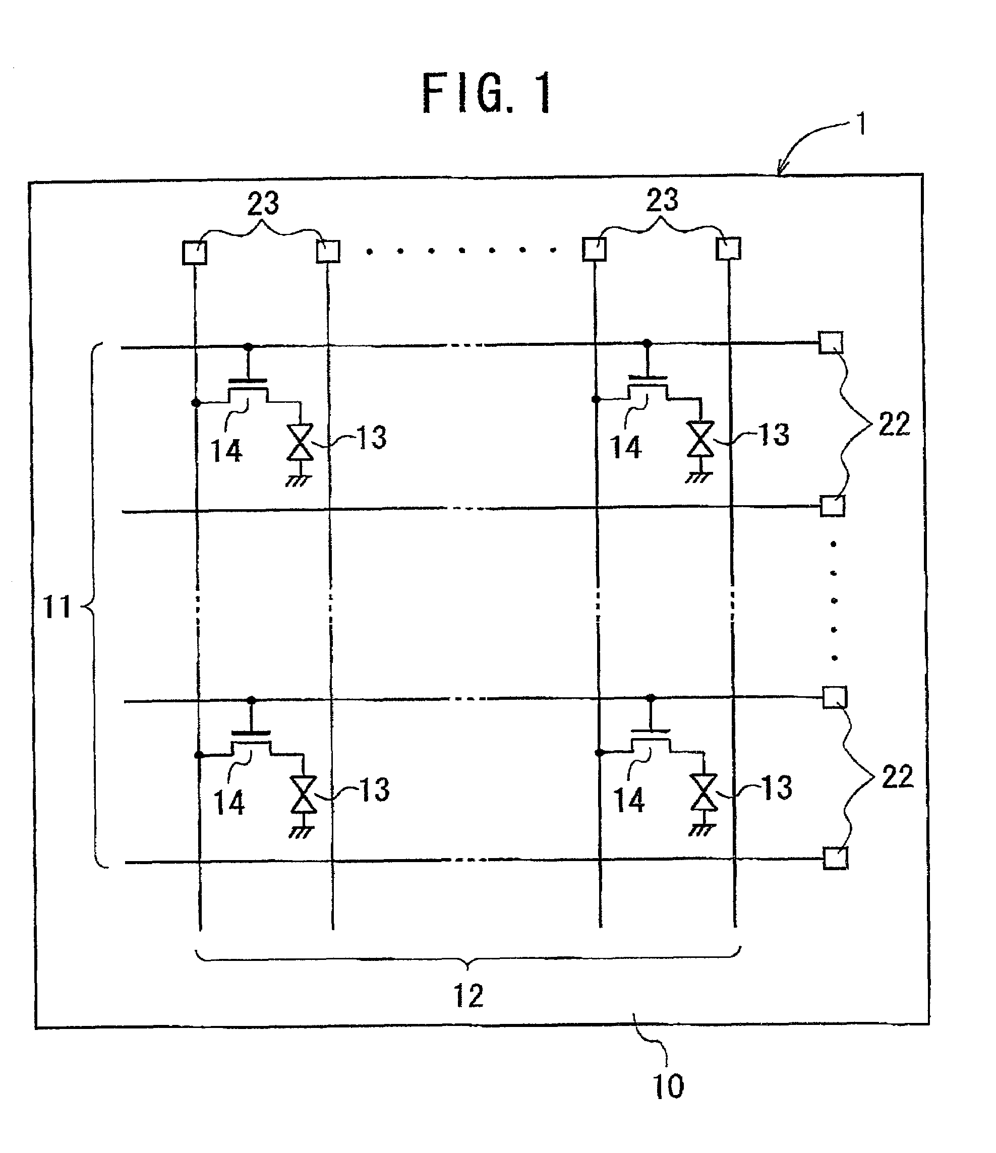
[0118]As shown in FIG. 1, the LCD device according to the first embodiment comprises an active matrix substrate 1 and an opposite substrate (not shown) coupled to each other in parallel to form a specific gap between them with a sealing member (not shown). The gap between the substrates forms a closed space in which a specific liquid crystal is confined. This configuration itself is known well and therefore, no further explanation is presented here.

[0119]Since the feature of the invention resides in the active matrix substrate 1, the following explanation will be mainly made with respect to the substrate 1. The substrate 1 has the following configuration.

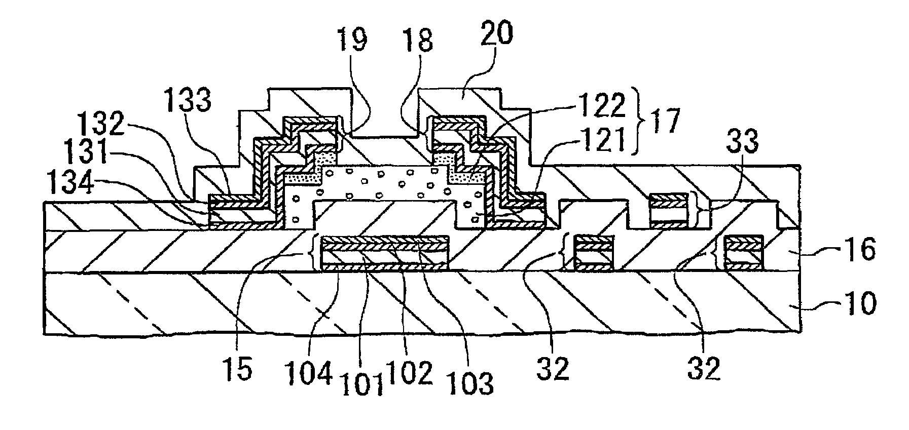
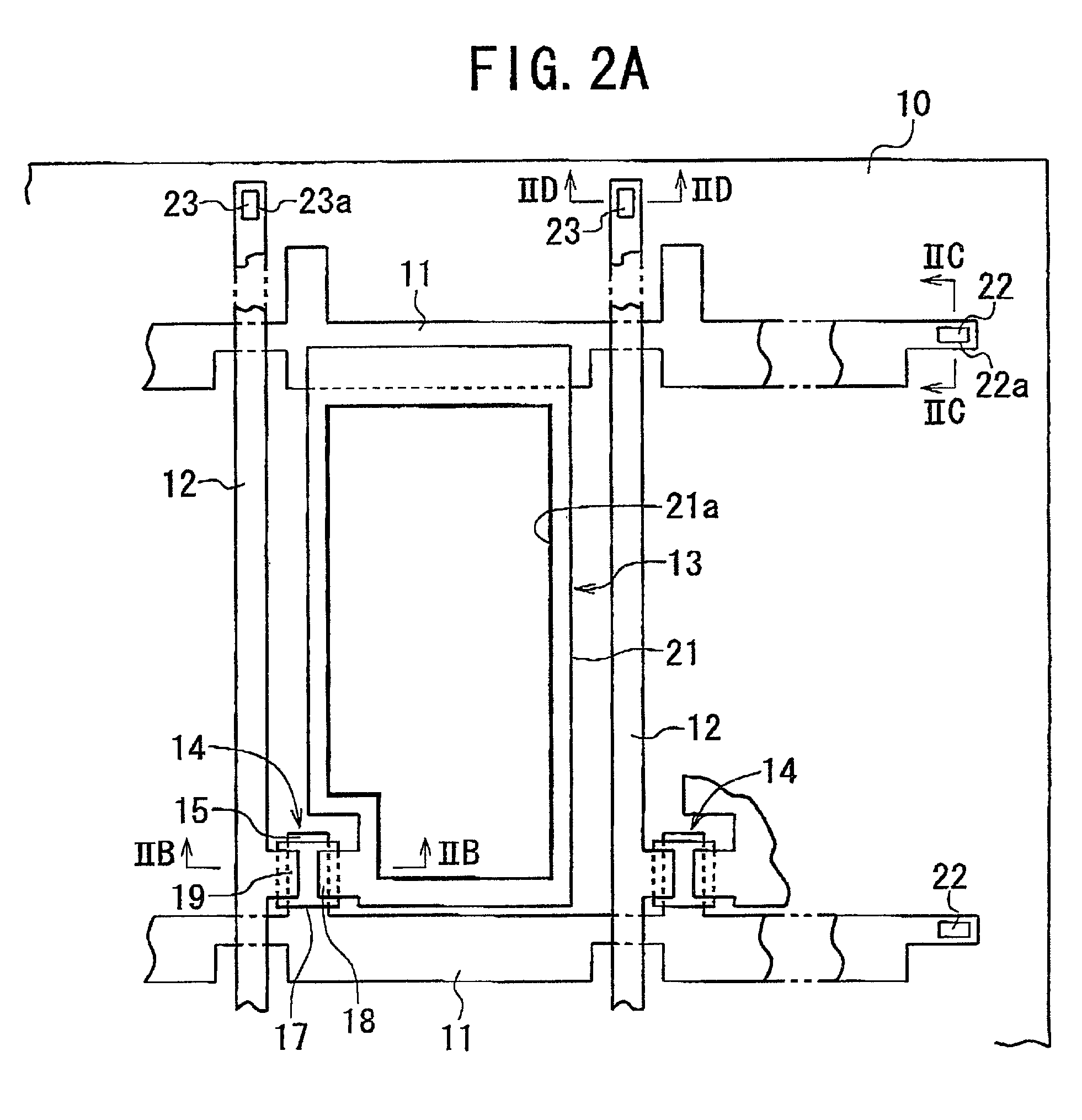
[0120]As shown in FIG. 1, the active matrix substrate 1 comprises a transparent glass plate 10. Scan lines 11 extending in the first direction (in the...

second embodiment

[0163]FIG. 10 and FIGS. 11A to 11E show the configuration of an active matrix substrate 1A used in an active matrix addressing LCD device according to a second embodiment of the invention. Unlike the first embodiment, this device is of the lateral electric-field type. This device comprises the active matrix substrate 1A and an opposite substrate (not shown) coupled to each other in parallel to form a specific gap between them-with a sealing member (not shown) The gap between the substrates forms a closed space in which a specific liquid crystal is confined. This configuration is the same as the first embodiment.

[0164]The same reference numerals or symbols are attached to the same or corresponding elements as those of the first embodiment in FIG. 10 and FIGS. 11A to 11E.

[0165]As shown in FIGS. 10 and 11A, the active matrix substrate 1A of the second embodiment comprises a transparent glass plate 10. Scan lines 11 extending in the first direction (in the horizontal direction in FIG. 1...

third embodiment

[0196]Although not illustrated here, an active matrix substrate used in an active matrix addressing LCD device according to a third embodiment has a three-level TiN / Al / Ti structure. Examples of the thickness of these Ti, Al, and TiN films are shown by the sample Nos. 5 and 6 in FIG. 7. The other configuration of the active matrix substrate of the third embodiment is the same as the substrate 1 of the first embodiment.

[0197]As seen from FIG. 7, the substrate of the third embodiment has an additional advantage that the number of Al hillocks can be made substantially zero, in other words, Al hillocks can be prevented approximately completely.

Variations

[0198]Needless to say, the invention is not limited to the above-described first to third embodiments. Any change or modification may be added to these embodiments within the spirit of the invention. For example, although a substantially pure Al film is used in the first to third embodiments, the invention is not limited to this. Any Al a...


PUM

PropertyMeasurementUnit
thicknessaaaaaaaaaa
thicknessaaaaaaaaaa
thicknessaaaaaaaaaa

Abstract

An active matrix addressing LCD device having an active matrix substrate on which conductive lines are formed is provided, which suppress the AI hillock without complicating the structure of the lines and which decreases the electrical connection resistance increase at the terminals of the lines, thereby improving the connection reliability. The device comprises an active matrix substrate having a transparent, dielectric plate, thin-film transistors (TFTs) arranged on the plate, and pixel electrodes arranged on the plate. Gate electrodes of the TFTs and scan lines have a first multilevel conductive structure. Common electrodes and common lines may have the first multilevel conductive structure. Source and drain electrodes of the TFTs and signal lines may have a second multilevel conductive structures. Each of the first and second multilevel conductive structures includes a three-level TiN/Ti/Al or TiN/Al/Ti structure or a four-level TiN/Ti/AI/Ti structure. Each of the TiN film of the first and second structures has a nitrogen concentration of 25 atomic % or higher. The Al file may be replaced with an Al alloy.

Description

BACKGROUND OF THE INVENTION[0001]1. Field of the Invention[0002]The present invention relates to an active-matrix addressing Liquid-Crystal Display (LCD) device having a so-called active-matrix substrate on which pixel electrodes and Thin-Film Transistors (TFTs) are arranged in a matrix array.[0003]More particularly, the invention relates to an active-matrix addressing LCD device with an active-matrix substrate on which multilayer-structured conductive lines are formed along with pixel electrodes and TFTs, which suppresses effectively aluminum (Al) hillocks without any complicated conductive line structure to thereby decreasing the connection resistance increase of the lines due to heat or moisture and improving their connection reliability.[0004]2. Description of the Related Art[0005]The active-matrix addressing LCD device has a typical configuration as follows.[0006]The LCD device of this type comprises an active matrix substrate and an opposite substrate coupled to each other in ...

Claims


Application Information

Patent Timeline
Patent Type & Authority Patents(United States)
IPC IPC(8): G02F1/1343G02F1/1345G02F1/136G02F1/1362G02F1/1368H01L29/45H01L29/49
CPCG02F1/13458G02F1/136286H01L29/458H01L29/4908G02F2001/13629G02F2001/136295G02F1/13629G02F1/136295G02F1/136
Inventor TANAKA, HIROAKIFUJITA, AKIRAKIMURA, SHIGERUMAEDA, AKITOSHIHAYASE, TAKASUKE
Owner NEC LCD TECH CORP
Why Eureka
Try Eureka