Supercharge Your Innovation With Domain-Expert AI Agents!

Semiconductor device and signal processing method for synchronizing data with a data strobe signal

a technology of synchronizing data and strobe signals, applied in the direction of generating/distributing signals, digital transmission, instruments, etc., can solve the problems of difficult simulation and verification of every feasible memory-mounted configuration, the flight times of data strobe signals and clock signals cannot be measured, and the design of memory controllers needs an extremely long time, etc., to achieve accurate determination of the valid range of data

Inactive Publication Date: 2010-03-09
SOCIONEXT INC
View PDF14 Cites 10 Cited by
  • Summary
  • Abstract
  • Description
  • Claims
  • Application Information

AI Technical Summary

Benefits of technology

The present invention relates to a semiconductor device that can accurately synchronize data with a system clock, regardless of the mounting and connection environments. The device includes a flight time acquisition unit that measures the time it takes for a clock signal and a data strobe signal to travel through a double-data-rate memory. A calculation unit then determines the valid range of data that needs to be synchronized with the system clock based on these flight times. Finally, a synchronizing unit synchronizes the data within this valid range. This invention ensures that data is always synchronized with the system clock, improving the overall performance and reliability of the semiconductor device.

Problems solved by technology

In circuit design of memory controller corresponded to DDR-SDRAM, DDR2-SDRAM and so forth, particular difficulties reside in a section allowing an internal flipflop to capture read data output from a memory, and a section taking part in synchronizing an output from the flipflop with a system clock.
A timing design therefor, however, needs simulation and verification with an accuracy of several tens to several hundreds of picoseconds, and therefore needs an extremely long time for delay design of the memory controller and timing design of printed circuit board (PCB).
It is therefore difficult to simulate and verify every feasible memory-mounted configurations, over the entire regions covering all variations in the manufacturing and temperature conditions.
The method is also disadvantageous in that it does not use an actual data strobe signal or a clock signal, and therefore does not conform to a geometry of an actual transmission path, so that flight times of the data strobe signal and the clock signal cannot be measured.
Adoption of the dummy read cycle load undesirably complicates the design of the memory controller-related components, and actual circuit operation cannot be bested unless the memory is connected.

Method used


Image

  • Semiconductor device and signal processing method for synchronizing data with a data strobe signal
  • Semiconductor device and signal processing method for synchronizing data with a data strobe signal
  • Semiconductor device and signal processing method for synchronizing data with a data strobe signal

Examples


Embodiment Construction

[0020]Paragraphs below will describe an embodiment of the present invention, referring to the attached drawings.

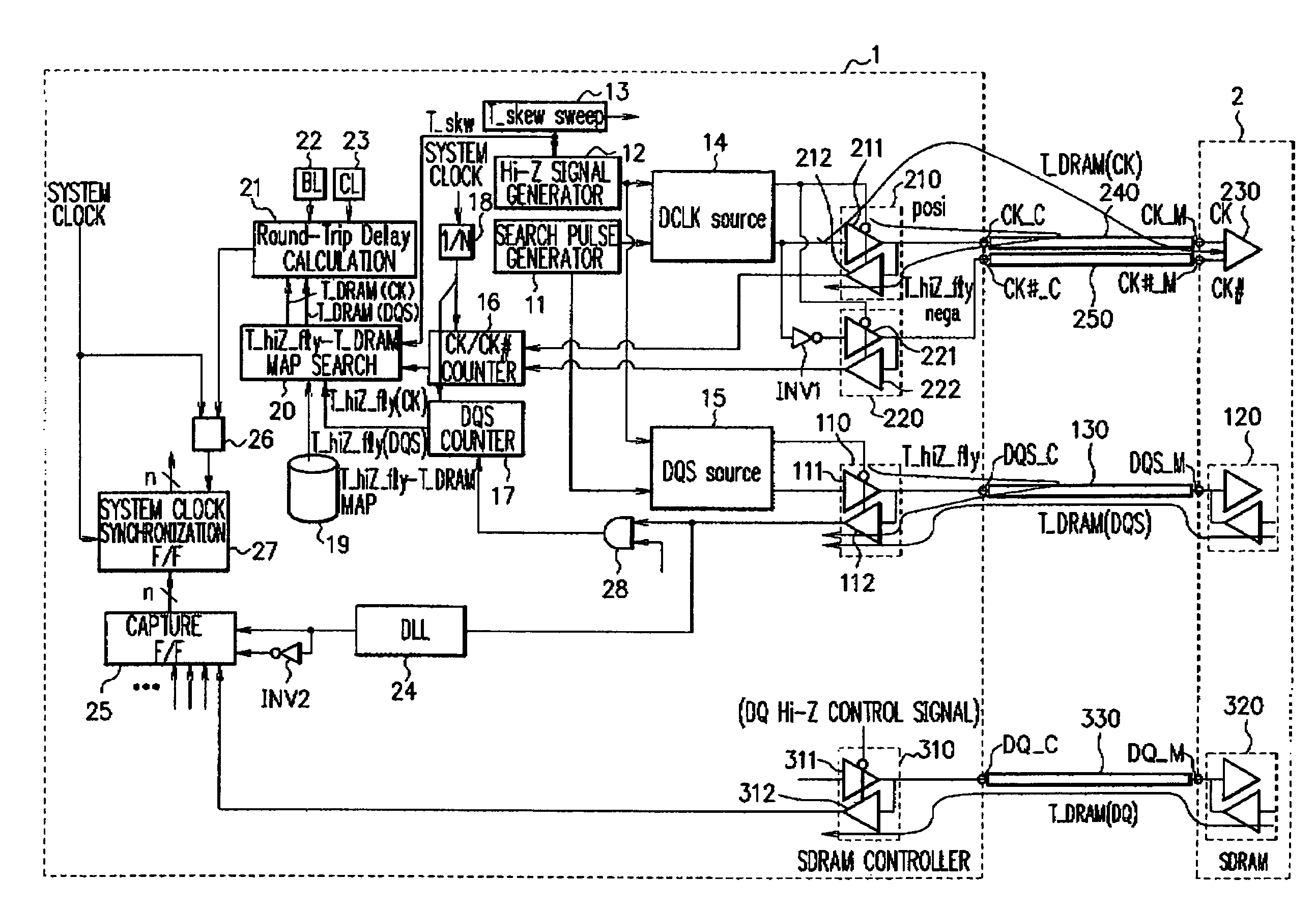
[0021]First an outline of a memory controller LSI applied with the semiconductor device according to an embodiment of the present invention will be explained.

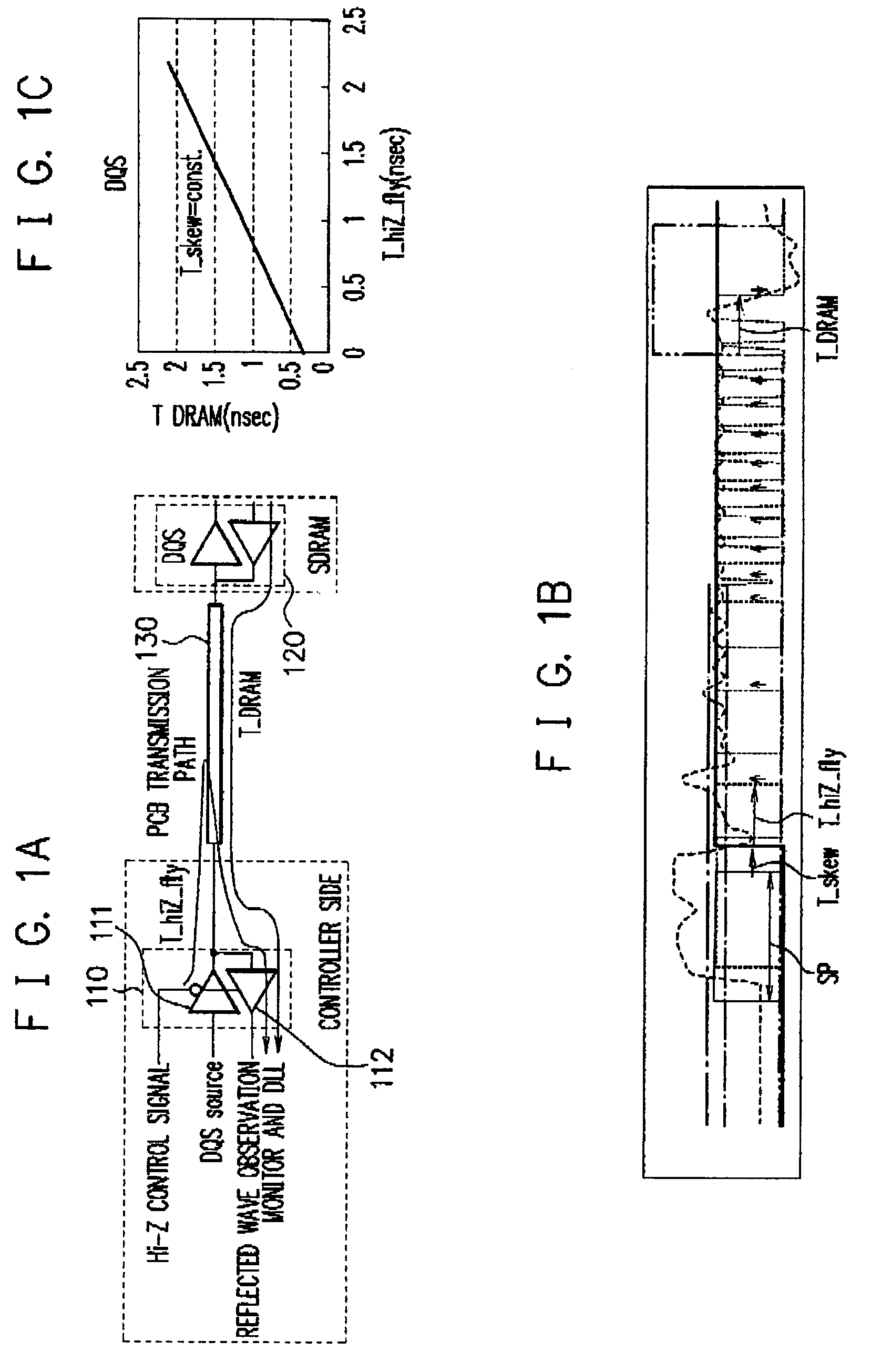
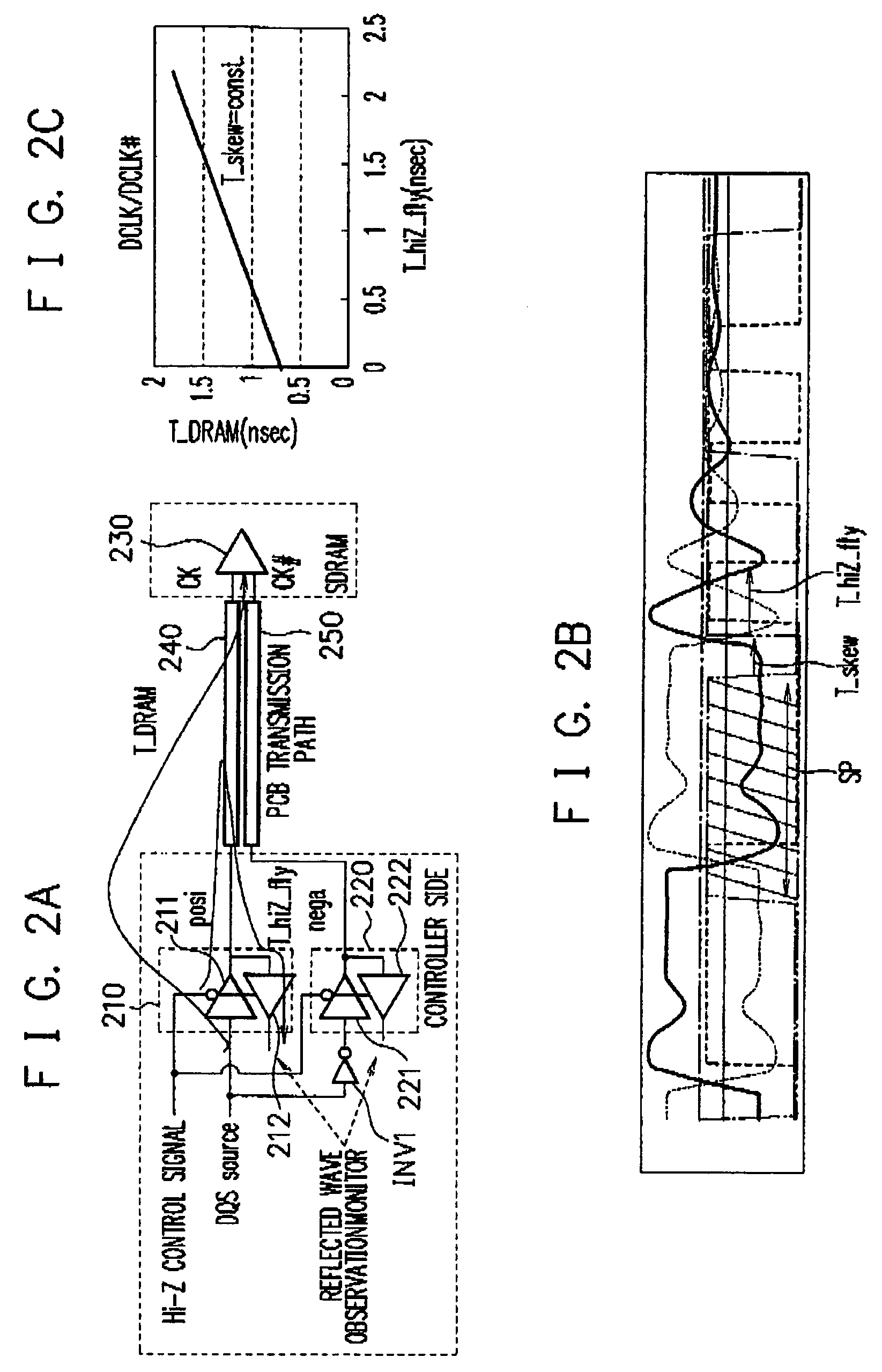
[0022]The memory controller LSI of this embodiment, as being mounted on a PCB board, delivers a search pulse on the actual PCB transmission paths (transmission paths respectively relevant to clock signals CK, CK# and a data strobe signal DQS), and measures a length of time up to detection of the reflected wave thereof. With respect to this process, the reflected wave is detected by using a bidirectional I / O (input / output circuit) so as to optimize a timing causative of skewing of the bidirectional I / O into a high-impedance state, and thereby creating a state of amplifying the reflected wave which appears on the PCB transmission path.

[0023]Next, the memory controller LSI determines the flight times of the actual clock ...


PUM


Abstract

In view of accurately determine a valid range of data to be synchronized to the system clock, conforming to actual environments of mounting and connection, the semiconductor device of the present invention is configured as acquiring flight times of clock signal(s) and a data strobe signal, transmitted to or from a double-data-rate memory, making use of reflected waves on transmission path, and as determining a valid range of data to be synchronized with a system clock based on thus-acquired flight times of the clock signal(s) and the data strobe signal.

Description

CROSS-REFERENCE TO RELATED APPLICATIONS[0001]This application is based upon and claims the benefit of priority from the prior Japanese Patent Application No. 2006-108996, filed on Apr. 11, 2006, the entire contents of which are incorporated herein by reference.BACKGROUND OF THE INVENTION[0002]1. Field of the Invention[0003]The present invention relates to a semiconductor device and a signal processing method, and in particular those preferably adoptable to a semiconductor device having an interface relevant to a double-data-rate (DDR) synchronous dynamic random access memory (SDRAM).[0004]2. Description of the Related Art[0005]In circuit design of memory controller corresponded to DDR-SDRAM, DDR2-SDRAM and so forth, particular difficulties reside in a section allowing an internal flipflop to capture read data output from a memory, and a section taking part in synchronizing an output from the flipflop with a system clock. In determination of a valid range of data to be synchronized, ...

Claims


Application Information

Patent Timeline
Patent Type & Authority Patents(United States)
IPC IPC(8): G06F1/12G06F1/00G06F1/04G06F13/00
CPCG06F13/1689G06F12/00G06F13/00
Inventor ANDO, NARUYOSHI
Owner SOCIONEXT INC
Features
  • R&D
  • Intellectual Property
  • Life Sciences
  • Materials
  • Tech Scout
  • Unparalleled Data Quality
  • Higher Quality Content
  • 60% Fewer Hallucinations
Learn More