Susceptor device

a technology of susceptor and surface, which is applied in the direction of coating, chemical vapor deposition coating, metallic material coating process, etc., can solve the problems of insufficient heat exchange between the plate sample and the temperature control section, the surface resist layer may burst, and the temperature on the surface may rise, etc., to achieve stable operability, reduce the interval, and improve the thermal conductivity and the transparency of the plasma

Inactive Publication Date: 2010-03-16
SUMITOMO OSAKA CEMENT CO LTD
View PDF18 Cites 400 Cited by
  • Summary
  • Abstract
  • Description
  • Claims
  • Application Information

AI Technical Summary

Problems solved by technology

For example, operations such as an etching operation are performed to the plate sample under a plasma atmosphere condition, temperature on a surface of the plate sample increase due to a heat which is caused in the plasma; thus, there may be a problem that a resist layer on the surface thereon may burst.
However, in the conventional susceptor device 1 as explained above, thickness of a ceramic supporting plate 3 is at least 3 mm; therefore, a heat is not sufficiently efficiently exchanged between the plate sample and the temperature controlling section 8.
Thus, there has been a problem in that it is difficult to maintain the plate sample at a constant preferable temperature.
Also, in the susceptor device 1, the thickness of the supporting plate 3 is at least 3 mm; therefore, there has been a problem in that it is difficult to generate a plasma stably because there is not a sufficient transparency for the plasma.
Also, in the susceptor device 1, there has been a concern that a heavy metal component in a bonding agent layer 9 may be volatile because the bonding agent layer 9 is not durable enough to a corrosive gas and a plasma.
Therefore, such a volatile heavy metal component may cause a contamination on the plate sample or become a source for generating a particle.
Furthermore, the bonding agent layer 9 is a conductive member; therefore, there has been a concern that there may occur an abnormal electric discharge on the bonding agent layer 9 when the bonding agent layer 9 is exposed to a plasma; thus there may occur a dielectric breakdown on the bonded surface.
Therefore, there has been a problem in that the susceptor device 1 does not work stably due to a frequent interruption by a safety device and a susceptor device 1 is not durable enough even if the susceptor device 1 works stably.

Method used


Image

  • Susceptor device
  • Susceptor device
  • Susceptor device

Examples


first embodiment

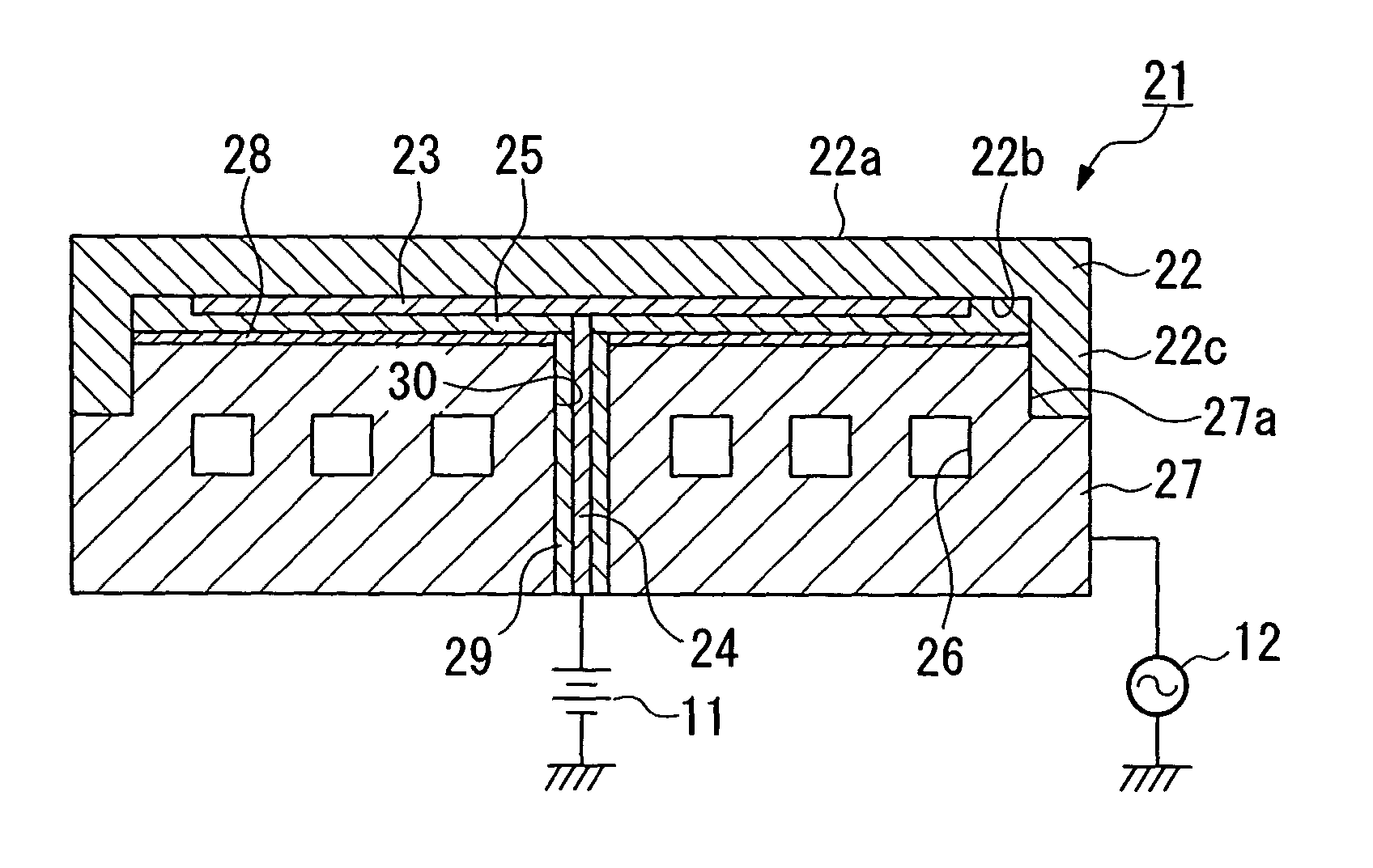
[0029]FIG. 1 is a cross section for showing a susceptor device according to a first embodiment of the present invention.

[0030]A susceptor device 21 comprises a base body 22 which is formed by a ceramic plate of which upper surface (a main surface) serves as a mounting surface 22a for mounting a plate sample such as a silicon wafer, an electrostatic absorbing inner electrode 23 having a predetermined pattern which is disposed on a bottom surface (other main surface) 22b of the base body 22, a power supplying terminal 24 one of which end section is connected to the electrostatic absorbing inner electrode 23 and another one of which end section is exposed to thereoutside, an insulating sprayed layer 25 which is fixed on the bottom surface 22b of the base body 22 so as to coat an entire surface of the electrostatic absorbing inner electrode 23 and a connecting section for the power supplying terminal 24 and the electrostatic absorbing inner electrode 23, and a temperature controlling se...

second embodiment

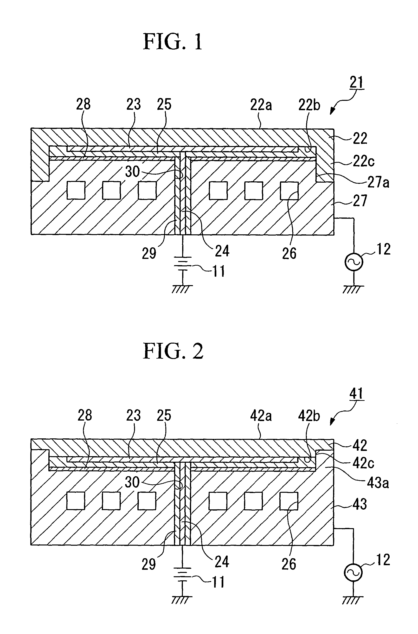
[0053]FIG. 2 is a cross section for the susceptor device according to a second embodiment of the present invention. A susceptor device 41 according to the second embodiment is different from the susceptor device 21 according to the first embodiment in following features. That is, in the susceptor device 21 in the first embodiment, a ring flange 22c is disposed around a peripheral section of the base body 22. Additionally, a notched section 27a having a fitting shape for the ring flange 22c is formed around an upper periphery of the temperature controlling section 27. In contrast, in the susceptor device 41 in the present embodiment, a notched section 42c is formed around a lower periphery of a base body 42. Additionally, a ring flange 43a having a fitting shape for the notched section 42c is disposed around an upper peripheral section of a temperature controlling section 43 such that the ring flange 43a on the temperature controlling section 43 is fitted to the notched section 42c o...

example

[0059]Here, examples are explained for explaining details for the present invention as follows.

[0060]Here, the susceptor device 21 which is shown in FIG. 1 is produced.

Manufacturing a Base Body

[0061]A mixture of 5 weight % of silicon carbide powder and aluminum oxide powder for the rest of the weight % is formed in to an approximate round plate. After that, the approximate round plate is sintered at a predetermined temperature; thus, an approximate round plate made of silicon carbide-aluminum oxide (alumina) sintered-composite is formed having 230 mm diameter and 1 mm thickness. Consequently, an upper surface (a main surface) of the sintered-composite is ground such that a flatness of the upper surface should be fewer than 10 μm so as to form a mounting surface on which the plate sample is supposed to be mounted. Thus, a ceramic base body 22 is formed.

Forming an Electrostatic Absorbing Inner Electrode

[0062]A mixture of 74.3 weight % of silver (Ag) powder, 21.0 weight % of copper (Cu...


PUM

PropertyMeasurementUnit
thicknessaaaaaaaaaa
thicknessaaaaaaaaaa
thicknessaaaaaaaaaa

Abstract

A susceptor device comprises a base body, an electrostatic absorbing inner electrode which is disposed on a bottom surface of the base body, a power supplying terminal, an insulating sprayed layer which coats the electrostatic absorbing inner electrode and a connecting section for the power supplying terminal and the electrostatic absorbing inner electrode, and a temperature controlling section. The insulating sprayed layer and the temperature controlling section are attached together unitarily via the bonding agent layer. The flange of the base body fits to a notched section of the temperature controlling section such that the electrostatic absorbing inner electrode, insulating sprayed layer, and the bonding agent layer should be sealed from thereoutside. It is possible to form a thin supporting plate and improve controllability for temperature on the plate sample and transparency for the plasma.

Description

[0001]Priority is claimed on Japanese Patent Application No. 2002-234078, filed Aug. 9, 2002, the content of which is incorporated herein by reference.BACKGROUND OF THE INVENTION[0002]1. Field of the Invention[0003]The present invention relates to a susceptor device which is used for fixing a plate sample such as a silicon wafer preferably in a semiconductor manufacturing device for manufacturing a semiconductor device such as an IC (Integrated Circuit), an LSI (Large Scale Integration), and a VLSI (Very Large-Scale Integration). In particular, the present invention relates to a susceptor device which fixes the plate sample by an electrostatic force while supporting the plate sample efficiently in a constant temperature so as to perform various operations such as a plasma-operation.[0004]2. Description of Related Art[0005]Conventionally, in manufacturing processes for manufacturing a semiconductor device such as an IC, an LSI, and a VLSI, the plate sample such as a silicon wafer is ...

Claims


Application Information

Patent Timeline
Patent Type & Authority Patents(United States)
IPC IPC(8): C23C16/00H01L21/68H01L21/00H01L21/3065H01L21/205H01L21/683
CPCH01L21/67103H01L21/67109H01L21/6831
Inventor MAKI, KEIGO
Owner SUMITOMO OSAKA CEMENT CO LTD
Why Eureka
Try Eureka