Press-fit integrated circuit package involving compressed spring contact beams

Active Publication Date: 2010-03-23
IXYS INTL LTD
View PDF8 Cites 13 Cited by
  • Summary
  • Abstract
  • Description
  • Claims
  • Application Information

AI Technical Summary

Benefits of technology

[0009]In one example, the novel integrated circuit package is used to package a microcontroller in an ultra low cost hand held infrared (IR) remote control device such as the type of remote control device used in the home to control electronic consumer devices such as televisions. Manufacturing of the hand held infrared remote control device is often extremely cost sensitive, and avoiding the cost of gold wire bonds and avoiding the costs associated with providing flip-chip bond bumps is particularly desirable in the remote control device application because achieving low manufacturing cost is very important but achieving high reliability of the device is less important. (The guaranteed usable lifetime of the remote control device may, for example, be less than ten years.) The spring contact beam portions of the lead can make direct contact with standard aluminum pads on the integrated circuit die, where these aluminum pads could, if the die were packaged in another type of package, be utilized for standard gold wire bond attachment to a leadframe. A single integrated circuit design is therefore usable both in the novel press-fit package as well as in a standard gold wire bonded package.

Problems solved by technology

Performing the wire bonding step in the above-described packaging process involves cost.
There are many different variations of flip-chip bonding, and the technique works well, but there are costs to using the technique.
Carrying out the extra bump-forming steps therefore involves an expense.
Moreover, there are often licensing payments that must be made and intellectual property issues that must be addressed in order to use many flip-chip packaging processes.
Bare integrated circuit dice can be directly reflow soldered to printed circuit boards of electronic consumer devices without integrated circuit packages, but this generally involves the semiconductor manufacturer losing control of the dice and can introduce reliability problems.
For example, solvents used to clean printed circuit boards in printed circuit board assembly houses, if such solvents come into contact with bare semiconductor dice, can compromise the dice and affect the future reliability of the dice.

Method used


Image

  • Press-fit integrated circuit package involving compressed spring contact beams
  • Press-fit integrated circuit package involving compressed spring contact beams
  • Press-fit integrated circuit package involving compressed spring contact beams

Examples


second embodiment

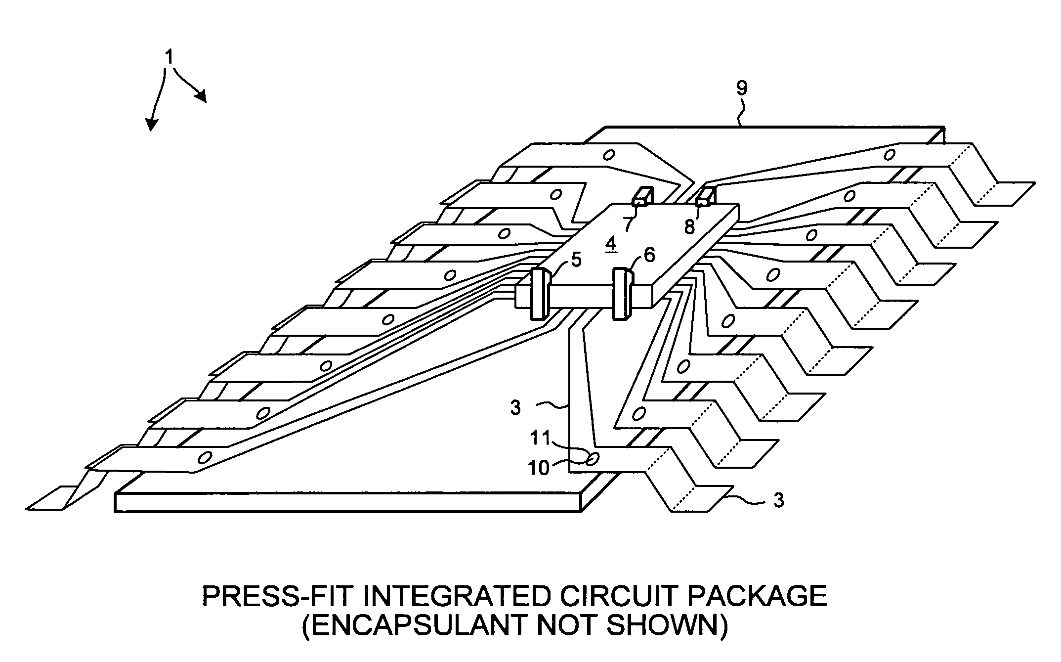
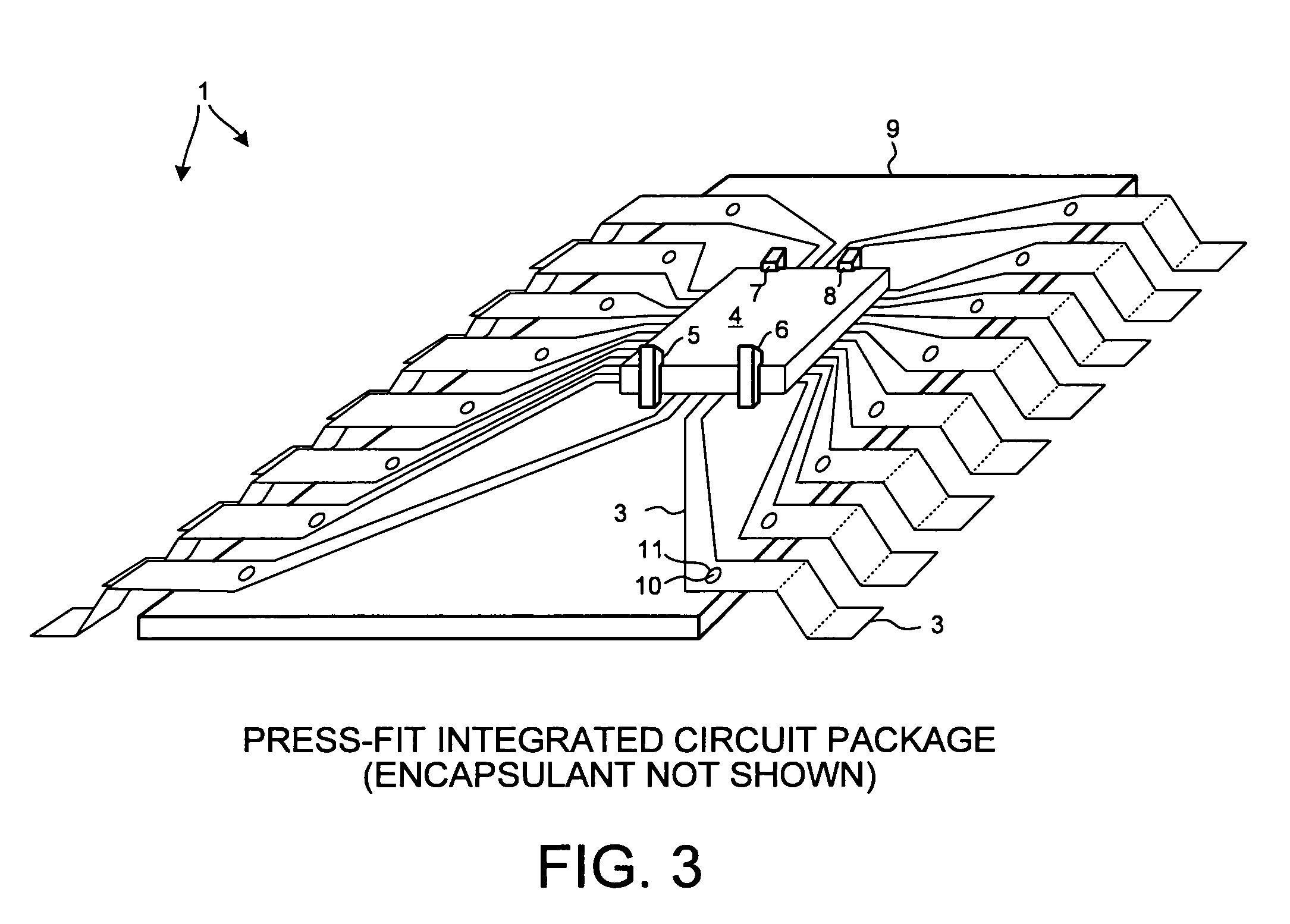
[0036]FIG. 10 is a top-down diagram of the leads and substrate and integrated circuit of a In this embodiment, the pins of the substrate are not thermally-welded to hold the leads in place. The leads do not have holes for accommodating such pins. Rather, the leads of the leadframe press-fit into a second set of retaining clips. Each lead in the diagram is held on two sides by a retaining clip. For example, lead 3 is held in place by retaining clips 26 and 27. The spring contact beam portion ends of the leads are held in place in the lateral dimension by guide slots in guide rails. FIG. 11 is a perspective view of guide slots in the guide rail 28 of FIG. 10. Lead 3 extends through guide slot 29. The spring contact beam portion ends of the leads are held down by integrated circuit 4. Accordingly, in the embodiment of FIG. 10, the leads are attached to the substrate in a press-fit mechanical pressing operation without the use of adhesives or thermal welding.

third embodiment

[0037]FIG. 12 is a cross-sectional diagram of a portion of a In this embodiment, injection molded substrate 9 includes an indentation 30. Integrated circuit 9 is placed in the indentation face side up. The leadframe is attached to the substrate so that the spring contact beams bend downward into the indentation. The leadframe is pressed down onto substrate 9, and the tops of the alignment and retaining pins of substrate 9 are melted to form the mushroom shape and to fix the leads to substrate 9. The cut and bending step is then performed to singulate the leads from each other and to form the outward ends of the leads into the desired shape. Die 4 is held in place by the pressing action of the spring contact beam portions without the use of flexible plastic retaining clips extensions of substrate 9.

fourth embodiment

[0038]FIG. 13 is a cross-sectional diagram of a portion of a In this embodiment, integrated circuit die 4 is not disposed in an indentation in substrate 9, rather the leads are formed such that they extend upward and over the edge of the upper face side of the die. The die 4 is disposed on the upper planar major surface of substrate 9 as illustrated. Die 4 is held in place by the pressing action of the spring contact beam portions without the use of flexible plastic retaining clips extensions of substrate 9.

[0039]Although certain specific embodiments are described above for instructional purposes, the teachings of this patent document have general applicability and are not limited to the specific embodiments described above. The die retaining clips may be disposed at the four corners of the die cavity, to hold down the four corners of the die, as opposed to the placement illustrated in FIG. 3. A die retaining clip may extend along substantially the entire length of a side of the di...


PUM


Abstract

An insulative substrate includes a plurality of flexible retaining clips and a plurality of alignment and retaining pins. A metal leadframe includes a plurality of leads. Each lead terminates in a spring contact beam portion. The leadframe is attached to the substrate (for example, by fitting a hole in each lead over a corresponding alignment and retaining pin and then thermally deforming the pin to hold the lead in place). An integrated circuit is press-fit down through the retaining clips such that pads on the face side of the integrated circuit contact and compress the spring contact beams of the leads. After the press-fit step, the retaining clips hold the integrated circuit in place. The resulting assembly is encapsulated. In a cutting and bending step, the leads are singulated and formed to have a desired shape. The resulting low-cost package involves no wire-bonding and no flip-chip bond bump forming steps.

Description

TECHNICAL FIELD[0001]The described embodiments relate to integrated circuit packaging.BACKGROUND INFORMATION[0002]Many different methods are known for packaging integrated circuits. In one method, an integrated circuit is die bonded face-side up to a metal leadframe. The leadframe is made of stamped metal and includes a plurality of radially extending leads. The leadframe is one leadframe of many in a strip of leadframes. The leads of each leadframe are held together by rails of metal material. Once the integrated circuit is attached to the center of the leadframe, each individual bond pad on the integrated circuit is typically wire bonded to the tip of an associated one of the radially extending leads. After the wire-bonding process is completed, a plastic encapsulant is injection molded around the die and wire bonds such that the leads extend outward from the plastic. After the plastic has hardened, the rails are typically cut away to singulate the leads from one another and to se...

Claims


Application Information

Patent Timeline
IPC IPC(8): H01L23/52H01L23/48H01L23/485H01L23/495H01L29/40H01L23/498
CPCH01L23/13H01L23/49506H01L23/49541H01L24/72H01L24/90H01L23/49811H01L24/05H01L2224/16H01L2224/48091H01L2224/48247H01L2924/01013H01L2924/01029H01L2924/01077H01L2924/01079H01L2924/01082H01L2924/01327H01L2924/14H01L2924/00014H01L24/48H01L2924/01005H01L2924/01006H01L2924/01033H01L2924/01047H01L2924/01074H01L2924/014H01L2224/45144H01L2924/00H01L2924/15747H01L24/45H01L2224/0401H01L2224/73251H01L2224/81901H01L2924/181H01L2224/72
Inventor STORTINI, THOMASRANSOM, JOHN A.
Owner IXYS INTL LTD
Why Eureka
Try Eureka