Organic electroluminescent display device having electrical communication between conducting layer and cathode layer
a display device and conductor technology, applied in semiconductor devices, semiconductor/solid-state device details, electrical apparatus, etc., can solve problems such as related art devices, and achieve the effect of significantly reducing the resistance of scan lines
- Summary
- Abstract
- Description
- Claims
- Application Information
AI Technical Summary
Benefits of technology
Problems solved by technology
Method used
Image

Examples
first embodiment
[0044]FIG. 2a is a plane view illustrating a light emitting display device according to the present invention. In FIG. 2a, an organic electroluminescent display is illustrated for explanation purposes. However, the invention is not limited to organic electroluminescent displays.
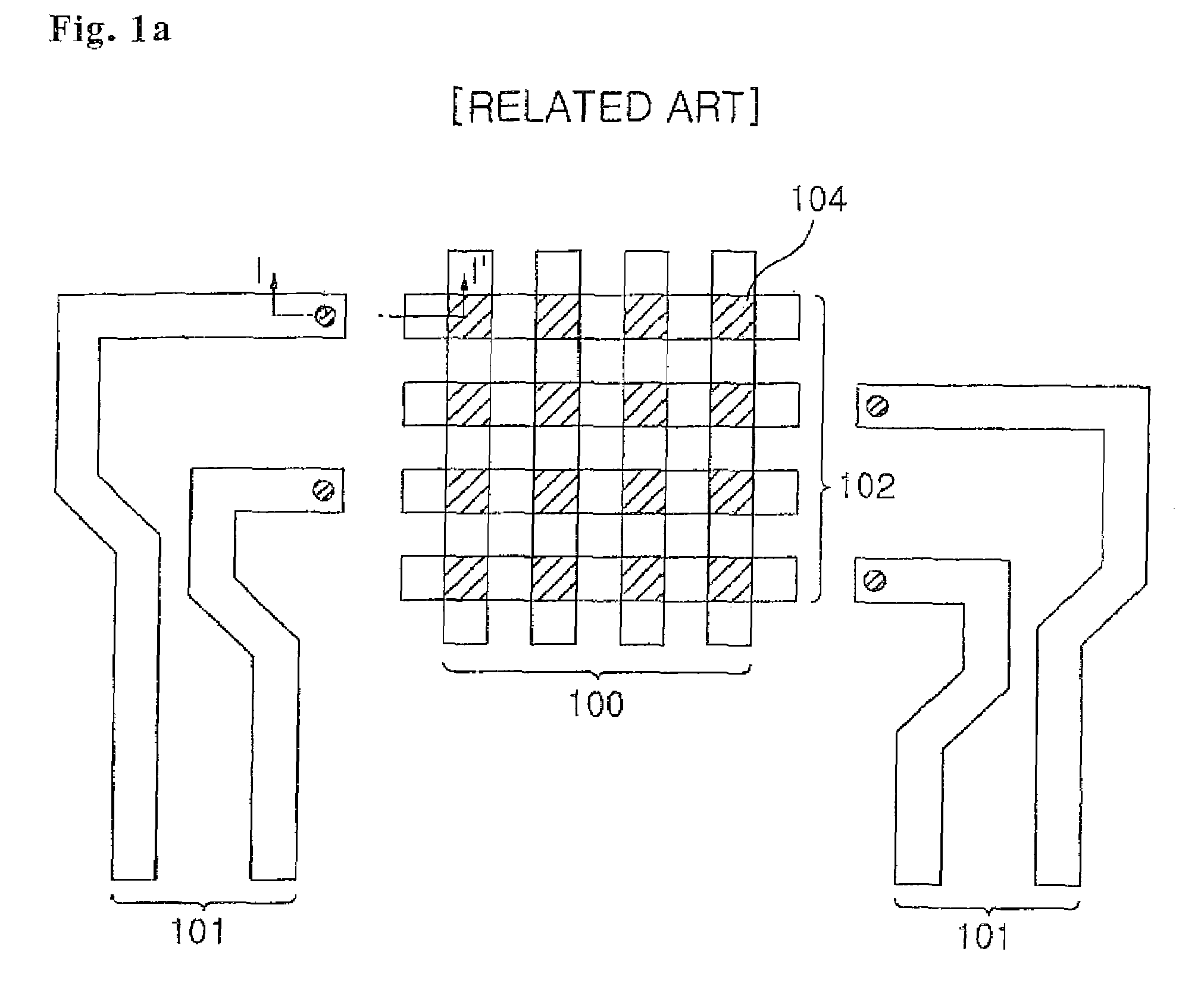
[0045]As shown in FIG. 2a, the organic electroluminescent device embodiment of the present invention includes anode electrode layers 200, cathode electrode layers 202 and scan lines 201.
[0046]A plurality of pixels 204 are formed in luminescent areas at the crossings of the anode electrode layers 200 and the cathode electrode layers 202. ITO layers are preferred to form the anode electrode layers 200, and metal layers are preferred to form the cathode electrode layers 202. The pixels 204 emit light when a sufficient voltage differential exists between the corresponding anode electrode layer 200 and the cathode electrode layer 202. For example, a positive voltage may be applied to the anode electrode layers 200...
second embodiment
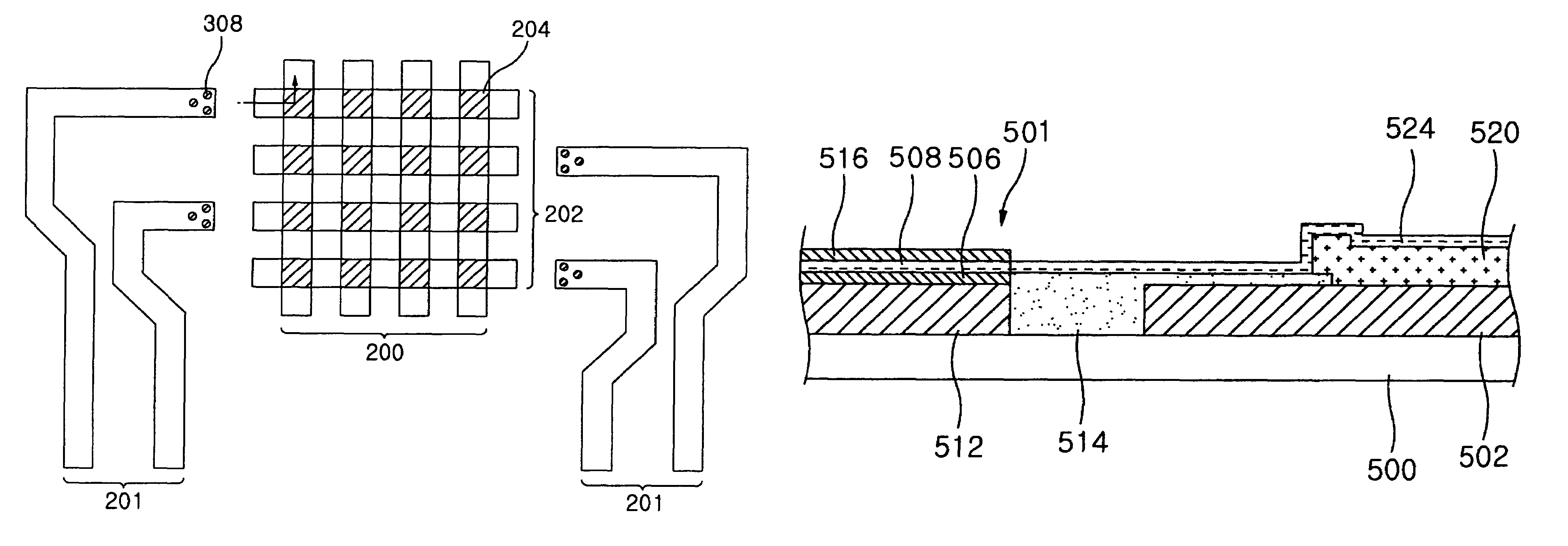
[0059]FIG. 3 is a plane view illustrating a light emitting display according to the present invention. Again for explanatory purposes only, an organic electroluminescent device is illustrated. As shown, the organic electroluminescent device includes anode electrode layers 200, cathode electrode layers 202 and scan lines 201. The remaining elements are similar to the elements of FIG. 2a. Therefore, the description for them is omitted.
[0060]In FIG. 3, a plurality of via holes 308 are formed on each scan line 201 rather than a single via hole 208 (see FIGS. 2a and 2b). Thus, the total area of the conducting layer 216 exposed through the via holes 308, through which the cathode electrode layer 202 electrically communicates with the conducting layer 216, is larger than that of the first embodiment as illustrated in FIG. 2a. The second embodiment allows the the contact resistance value between the conducting layer 216 and the cathode electrode layer 202 to be lowered even further.
[0061]FI...
third embodiment
[0071]The manufacturing process of the organic electroluminescent device according to the present invention is as follows. The anode electrode layers 502 and scan lines 501 are formed spaced from each other on the substrate 500. The scan line 501 is formed by stacking the scan line electrode layer 512, the first sub-electrode layer 506, the conducting layer 508 and the second sub-electrode layer 516 in sequence. Here, aluminum may be used to form the conducting layer 508 and molybdenum or chrome may be used to form the first sub-electrode layer 506 and / or the second sub-electrode layer 516.
[0072]Then, the insulating layer is formed over the anode electrode layer 502. Luminescent areas on the anode electrode layer 502 are exposed by patterning the insulating layer.
[0073]The supporting layer 514 is formed by filling the space between the scan line 501 and the anode electrode layer 502 with the insulating layer 514. The supporting layer 514 is formed at the same height as the total hei...
PUM
 Abstract
Description
Claims
Application Information
 - R&D
- Intellectual Property
- Life Sciences
- Materials
- Tech Scout
- Unparalleled Data Quality
- Higher Quality Content
- 60% Fewer Hallucinations
Browse by: Latest US Patents, China's latest patents, Technical Efficacy Thesaurus, Application Domain, Technology Topic, Popular Technical Reports.
© 2025 PatSnap. All rights reserved.Legal|Privacy policy|Modern Slavery Act Transparency Statement|Sitemap|About US| Contact US: help@patsnap.com