

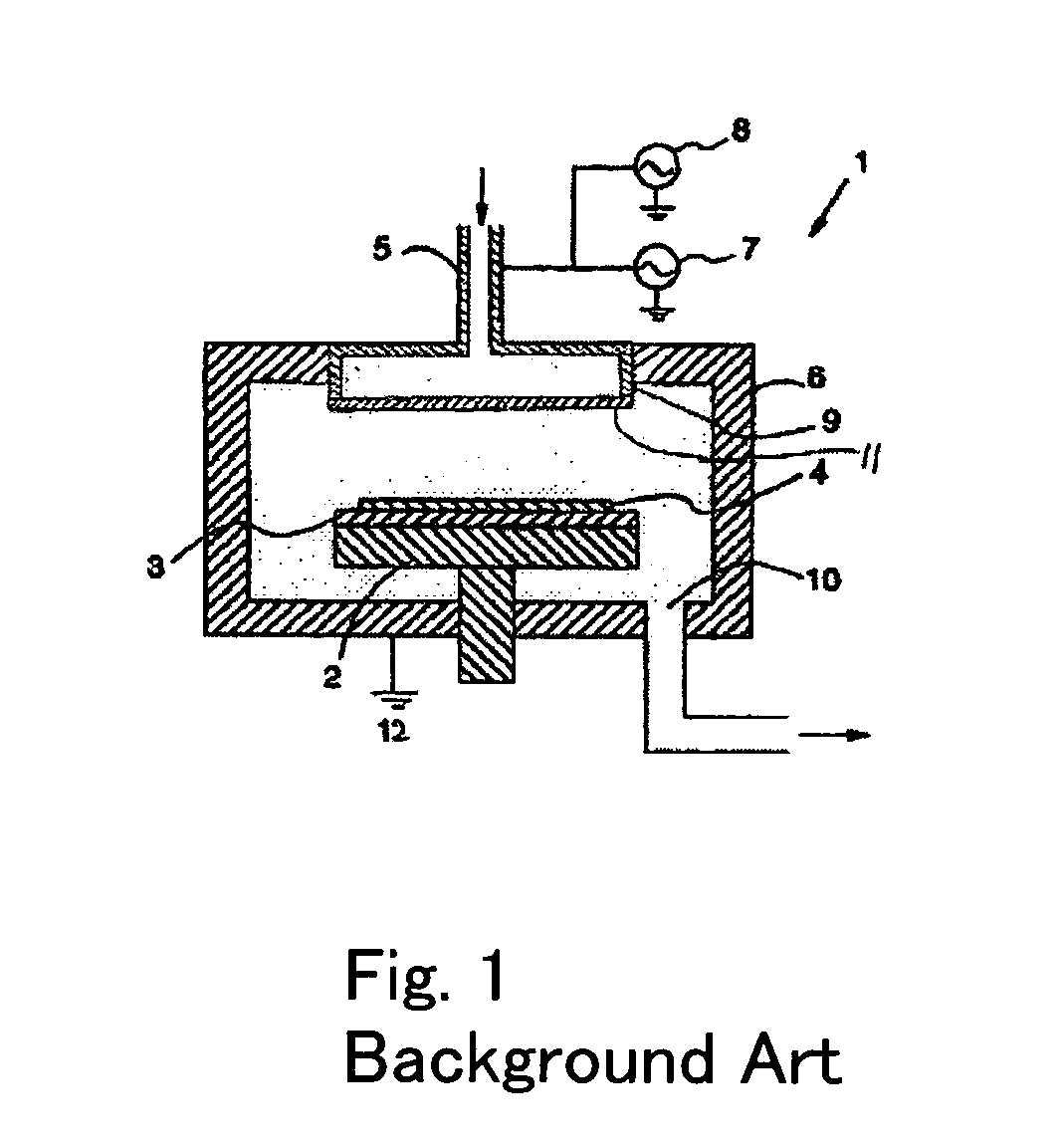
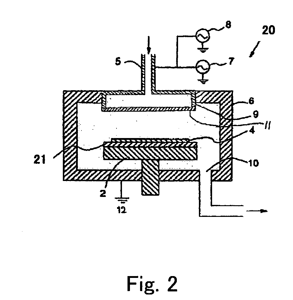
Substrate-supporting device
a support device and substrate technology, applied in vacuum evaporation coatings, chemical vapor deposition coatings, coatings, etc., can solve the problems of insufficient reduction, stress, and worsening of the uniformity of the thickness of the film within the film, so as to suppress the sticking of the workpiece (substrate) and control the surface state of the susceptor
- Summary
- Abstract
- Description
- Claims
- Application Information
AI Technical Summary
Benefits of technology
Problems solved by technology
Method used
Image

Examples
example
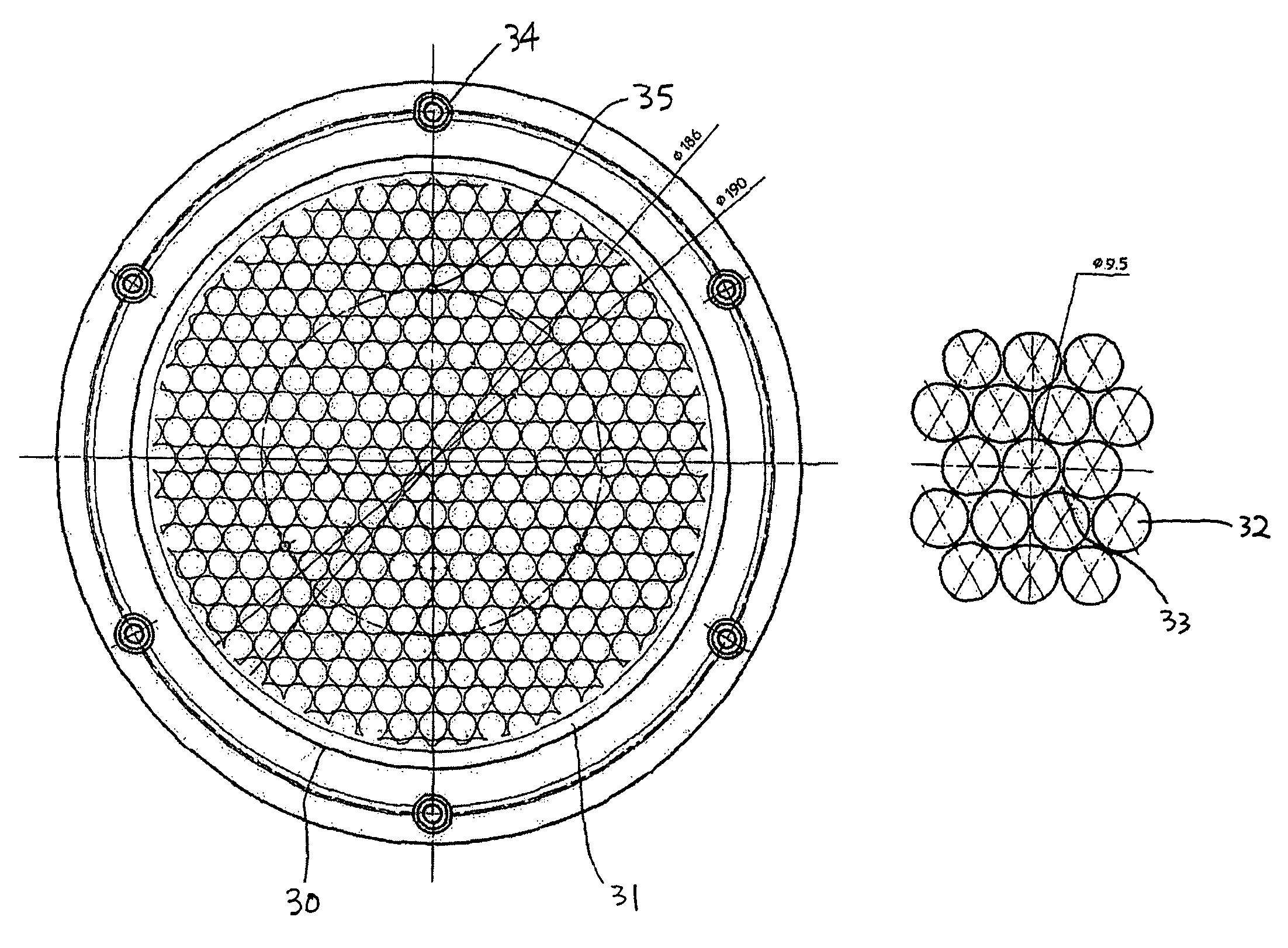
[0047]In this example, multiple circular dimples are disposed on a susceptor 21 as low regions for the reason of facilitating machining, etc. High regions are continuous. The susceptor is used for a φ200 mm wafer. A shape of the susceptor used in this example is shown in FIGS. 7(a)-(c). A depth of the circular dimple 32 is 0.2 mm; its inner diameter is 9.5 mm; a distance between the respective centers of circular adjacent dimples is 10 mm (consequently, a radial thickness is 0.5 mm). Additionally, every three dimples adjacent to each other are arranged such that imaginary lines connecting respective centers of the three circular shapes form an equilateral triangle (FIG. 7(b)). A side of the equilateral triangle is 10 mm.
[0048]Additionally, an outer diameter of the susceptor 21 is 250 mm; an outer diameter of a substrate-supporting region 31 is 201 mm; a width of a wafer pocket 31 is 6 mm; a height of a peripheral portion of the wafer pocket is 0.5 mm; an outer diameter of an area in...
experimental examples
[0052]Film type: TEOS
[0053]
Film FormationSource gas 1:TEOS (100 sccm)Source gas 2:O2 (1000 sccm)First RF power source (HRF):13.56 MHz (1.0 W / cm2 -Anode standard)Second RF power source (LRF):400 kHz (0.37 W / cm2)Substrate:φ200 mm silicon substrate
[0054]Result
[0055]FIG. 4 shows film formation results. FIG. 6 shows contact-area dependence of a wafer sticking ratio on a wafer and a susceptor when film deposition is carried out continuously on 10 pieces of wafers, each of which has both sides polished and the bottom surface coated with a silicon nitride film. Additionally, FIGS. 5(a)-(e) show mapping results of in-plane uniformity in each film. The reason why a silicon nitride film was coated on the bottom surface of a wafer with its both sides polished was to facilitate wafer sticking. As seen from uniformity values shown in FIG. 4 and mapping results shown in FIGS. 5(a)-(e), it is seen that the smaller a contact area of a wafer and a susceptor becomes, the more in-plane uniformity of fi...
PUM
| Property | Measurement | Unit |
|---|---|---|
| Ra | aaaaa | aaaaa |
| depth | aaaaa | aaaaa |
| temperature | aaaaa | aaaaa |
Abstract
Description
Claims
Application Information