Terminal for engaging type connector

a connector and type technology, applied in the direction of coupling contact members, superimposed coating processes, capacitors, etc., can solve the problems of inferior material solder-bonding properties to materials entirely coated with sn layers, and the improvement of such an improvement is not substantial, so as to achieve good bonding properties and reduce frictional properties , the effect of high surface roughness

Active Publication Date: 2010-04-20
KOBE STEEL LTD
View PDF9 Cites 13 Cited by
  • Summary
  • Abstract
  • Description
  • Claims
  • Application Information

AI Technical Summary

Benefits of technology

[0022]In the terminal in the first aspect of the present invention for an engaging type connector, parts of the Cu—Sn alloy layer coated with the Sn layer are exposed when the base material has a high surface roughness and the Sn layer is caused to flow and is smoothed by the reflowing process. It is desirable that the Cu—Sn alloy layer on the solder-bonding part is not exposed and the solder-bonding part is coated entirely with the Sn layer when the Cu—Sn alloy layer on the engaging part is partly exposed. Such a condition can be easily satisfied because the solder-bonding part has a surface roughness lower than that of the engaging part. Another plated Sn layer may be formed after the reflowing process to coat the surface entirely.
[0034]In the terminal in the second aspect of the present invention for an engaging type connector, the Cu—Sn alloy layer is partly exposed in the surface of the engaging part. Parts of the Cu—Sn alloy layer coated with the Sn layer are exposed when the base material has a high surface roughness and the Sn layer is caused to flow and is smoothed by the reflowing process. It is desirable that the Cu—Sn alloy layer on the solder-bonding part is not exposed when the Cu—Sn alloy layer on the engaging part is partly exposed. Even if the Cu—Sn alloy layer is exposed partly in the solder-bonding part, the degree of exposure of the Cu—Sn alloy layer in the solder-bonding part is less than that in the engaging part because the mean thickness of the Sn layer on the solder-bonding part is greater than that on the engaging part, and hence the solder-bonding property of the solder-bonding part is relatively excellent. When the Cu—Sn alloy layer on the engaging part is exposed partly after the reflowing process, the exposed parts of the Cu—Sn alloy layer may be coated with another Sn layer.
[0035]In the terminal having the engaging part and the solder-bonding part in each of the first and the second aspect of the present invention for an engaging type connector, the engaging part has a low frictional property, and the solder-bonding part has an improved solder-bonding property.
[0036]In the first aspect of the present invention, since the surface of the part corresponding to the engaging part of the base material is roughened desirably in an arithmetic mean roughness Ra of 0.15 μm or above at least with respect to one direction and in an arithmetic mean roughness Ra of 4.0 μm or below with respect to all directions, parts of the Cu—Sn alloy layer corresponding to the projections of the irregular surface of the base material are exposed or parts of the Sn layer corresponding to the projections in the roughened surface of the base material are very thin. Therefore, the engaging part has a low frictional property as compared with the ordinary material entirely coated with a Sn layer having a substantially uniform thickness even if the mean thickness is the same. The part corresponding to the solder-bonding part of the base material has a surface roughness as low as that of an ordinary Cu—Sn alloy layer alloy strip having an arithmetic mean roughness below 0.15 μm with respect to all directions and is coated entirely with the Sn layer having a substantially uniform thickness and hence the solder-bonding part is excellent in solder-bonding property.
[0037]According to the second aspect of the present invention, the Sn layer is the outermost layer, and the Cu—Sn alloy layer having a high hardness underlies the Sn layer. Since the mean thickness of the part corresponding to the solder-bonding part of the Sn layer is greater than that of the part corresponding to the engaging part of the Sn layer, the solder-bonding part has a relatively improved solder-bonding property. Since the part corresponding to the engaging part of the Sn layer is thin, the engaging part has a relatively improved frictional property. Particularly, the Cu—Sn alloy layer alloy strip, namely, the base material, has a surface roughness represented by an arithmetic mean roughness Ra of 0.15 μm or above at least with respect to one direction and an arithmetic mean roughness Ra of 4.0 μm or below with respect to all directions, and higher than that of an ordinary Cu—Sn alloy layer alloy strip, parts of the Cu—Sn alloy layer corresponding to the projections in the surface of the part corresponding to the engaging part of the base material are exposed or parts of the Sn layer corresponding to the projections in the surface of the part corresponding to the engaging part of the base material are thin, and the engaging part has a low frictional property. The mean thickness of the part corresponding of the solder-bonding part is greater than that of part corresponding to the engaging part, and the solder-bonding part is excellent in solder-bonding property. The solder bonding part is particularly excellent in solder-bonding property when the solder-bonding part is coated entirely with the Sn layer.

Problems solved by technology

Since parts of the Cu—Sn alloy layer are exposed in the surface of the material, the material is inferior in solder-bonding property to a material entirely coated with a Sn layer.
However those materials are unsatisfactory in solder-bonding property.
Although the improvement of the solder-bonding property can be achieved by the postplating process as mentioned in those patent documents, it goes without saying that such an improvement is not a substantial improvement.
When a thick plated Sn layer is formed by a postplating process to improve the solder-bonding property as mentioned in JP-A 2004-68026, friction increases and hence the material is not suitable for forming an engaging type terminal.

Method used


Image

  • Terminal for engaging type connector
  • Terminal for engaging type connector
  • Terminal for engaging type connector

Examples


first embodiment

[0051]A terminal in a first embodiment according to the present invention for an engaging type connector and a method of manufacturing the same will be described with reference to FIGS. 1 to 6.

[0052]The terminal, which is assumed to be a pin terminal for a printed wiring board, is manufactured by the following steps.

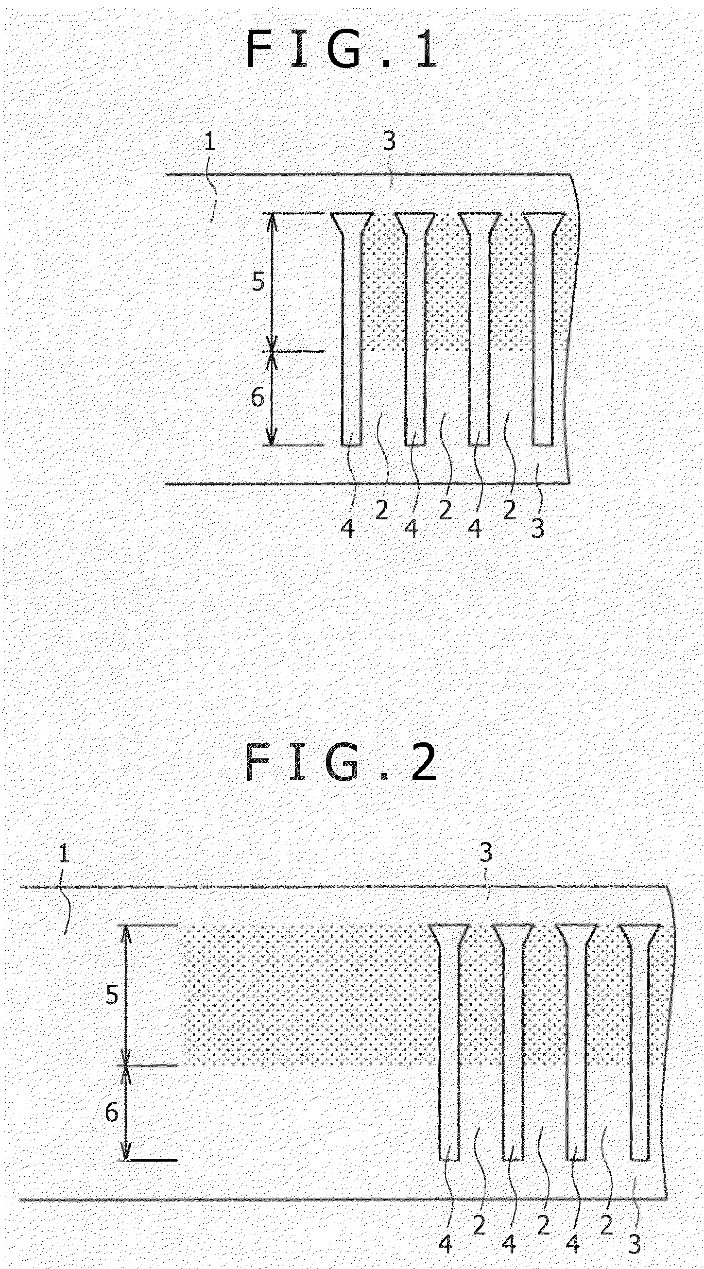
[0053](1) Referring to FIG. 1, a normally rolled Cu alloy strip 1 is subjected to a punching process by a progressive die to form longitudinally arranged terminal bodies 2 connected by connecting parts 3. Indicated at 4 are openings formed by the punching process.

[0054]The surfaces of engaging parts 5 of the terminal bodies 2 are roughened by press work concurrently with the punching process. In FIG. 1, parts shaded by small dots are engaging parts 5 having the rough surfaces. The surface roughness of solder-bonding parts 6 of the terminal bodies 2 are the same as the original surface roughness of the Cu alloy strip 1. The press work is executed before the Cu strip 1 is ...

second embodiment

[0075]A terminal in a second embodiment according to the present invention for an engaging type connector and a method of manufacturing the same will be described with reference to FIGS. 11 to 13, in which parts like or corresponding to those of the first embodiment are designated by the same reference characters.

[0076]The terminal, which is assumed to be a pin terminal for a printed wiring board, is manufactured by the following steps.

[0077](1) Referring to FIG. 11A, a Cu alloy strip 1 is subjected to a punching process to form longitudinally arranged terminal bodies 2 connected by connecting parts 3. The surface of the Cu alloy strip 1 has an arithmetic mean roughness Ra of 0.15 μm or above at least with respect to one direction and an arithmetic mean roughness Ra of 4.0 μm or below with respect to all directions. Indicated at 4 are openings formed by the punching process. FIG. 11A shows the Cu alloy strip 1 in a state after a postplating process.

[0078](2) The entire surface of th...

example 1

[0127]Example 1 of the present invention will be shown.

[0128]Preparation of Test Samples

[0129]Processes used for making test samples Nos. 1 to 31 are shown in Tables 1 and 2.

[0130]A Cu alloy plate containing Cu, 1.8% by mass Ni, 0.40% by mass Si, 0.10% by mass Sn and 1.1% by mass Zn was processed to provide base materials. The surface of the Cu alloy plate was roughened by using a work roll having a surface roughened by shot blasting for rolling (or not roughened) to provide base materials having a Vickers hardness 200, a thickness of 0.25 mm, and different surface roughnesses, respectively. The respective surface roughnesses of parts of the base materials corresponding to engaging parts of test samples are shown in Tables 3 and 4. The respective surface roughnesses Ra of parts of the base materials corresponding to solder-bonding parts of all the test samples Nos. 1 to 31 are 0.05 μm.

[0131]A plated Ni layer (or no plated Ni layer), a plated Cu layer (or no plated Cu layer) and a pl...


PUM

PropertyMeasurementUnit
heightaaaaaaaaaa
heightaaaaaaaaaa
heightaaaaaaaaaa

Abstract

A terminal for an engaging type connector includes a punched Cu alloy strip as a base material, a coating formed on the Cu alloy strip by postplating processes and including a Sn layer, and a Cu—Sn alloy layer sandwiched between the base material and the Sn layer. The Sn layer is smoothed by a reflowing process. The terminal has an engaging part and a solder-bonding part, and the surface of a part of the base material corresponding to the engaging part has a surface roughness higher than that of the surface of the base material corresponding to the solder-bonding part. The engaging part has a low frictional property and the solder-bonding part has improved solder wettability.

Description

BACKGROUND OF THE INVENTION[0001]1. Field of the Invention[0002]The present invention relates to a terminal, for an engaging type connector, having an engaging part and a solder-bonding part.[0003]2. Description of the Related Art[0004]Mentioned in JP-A 2006-77307 is a conducting material, for a connecting part, having high electrical reliability (low contact resistance) and a low frictional property, and suitable for forming a terminal for an engaging type connector. The technique disclosed in JP-A 2006-77307 uses a copper alloy strip having a surface roughness greater than that of ordinary copper alloy strips as a base material, forms a plated Ni layer, a plated Cu layer and a plated Sn layer in that order, forms a plated Cu layer and a plated Sn layer in that order, or forms only a plated Sn layer on the surface of the base material, processes the plated Sn layer by a reflowing process to form a Cu—Sn alloy layer by the plated Cu layer and the plated Sn layer, or by the copper al...

Claims


Application Information

Patent Timeline
Patent Type & Authority Patents(United States)
IPC IPC(8): H01B5/00
CPCC23C2/02C23C2/28C23C26/02C23C28/023C23C28/021C25D5/34C25D5/505H01R13/03C25D5/10C25D5/12
Inventor MASAGO, YASUSHIOZAKI, RYOICHITAIRA, KOUICHI
Owner KOBE STEEL LTD
Why Eureka
Try Eureka