Programmable delay line compensated for process, voltage, and temperature

a delay line and process technology, applied in the field of integrated circuit technology, can solve the problems of difficult design, noise, and difficult noise reduction of phase interpolators with good linearity characteristics, and achieve the effects of improving the design accuracy, and improving the design accuracy

Inactive Publication Date: 2010-04-20
MICROSEMI SOC
View PDF5 Cites 7 Cited by
  • Summary
  • Abstract
  • Description
  • Claims
  • Application Information

AI Technical Summary

Benefits of technology

[0012]A PVT-compensated delay element has a selectable amount of delay. According to one application, the delay element is placed in series with either the reference or feedback input to a phase-locked loop (PLL) to allow predictable time shifting of the PLL output by the selected amount of delay. Alternate uses are possible.

Problems solved by technology

Their use frequently results in delays that are not predictable and are thus often quite different from the ideally desired value.
First, like many analog circuits it can be harder to design and be more susceptible to noise than the equivalent digital function.
Phase interpolators with good linearity characteristics can be particularly difficult to design.
The '634 patent teaches using different numbers of coarse time delay units in different embodiments in applications requiring different degrees of time resolution, but a considerable degree of flexibility is lost by limiting the programmable control functionality exclusively to the slave delay line.
This introduces a non-PVT compensated delay term into the output delay that may be significant in some applications.
While multiple output phase (multi-phase) phase-locked loops (PLLs) and multi-phase DLLs are present on many FPGAs for clock applications, no general purpose PVT compensated programmable delay line suitable for use with both clocks and other signals has been previously disclosed.

Method used


Image

  • Programmable delay line compensated for process, voltage, and temperature
  • Programmable delay line compensated for process, voltage, and temperature
  • Programmable delay line compensated for process, voltage, and temperature

Examples


Embodiment Construction

[0028]Persons of ordinary skill in the art will realize that the following description of the present invention is illustrative only and not in any way limiting. Other embodiments of the invention will readily suggest themselves to such skilled persons.

[0029]Many PLL features (like input / output dividers) and FPGA features (like programmable connections to / from these blocks) known to persons of ordinary skill in the art have been omitted for the sake of simplicity and clarity of presentation.

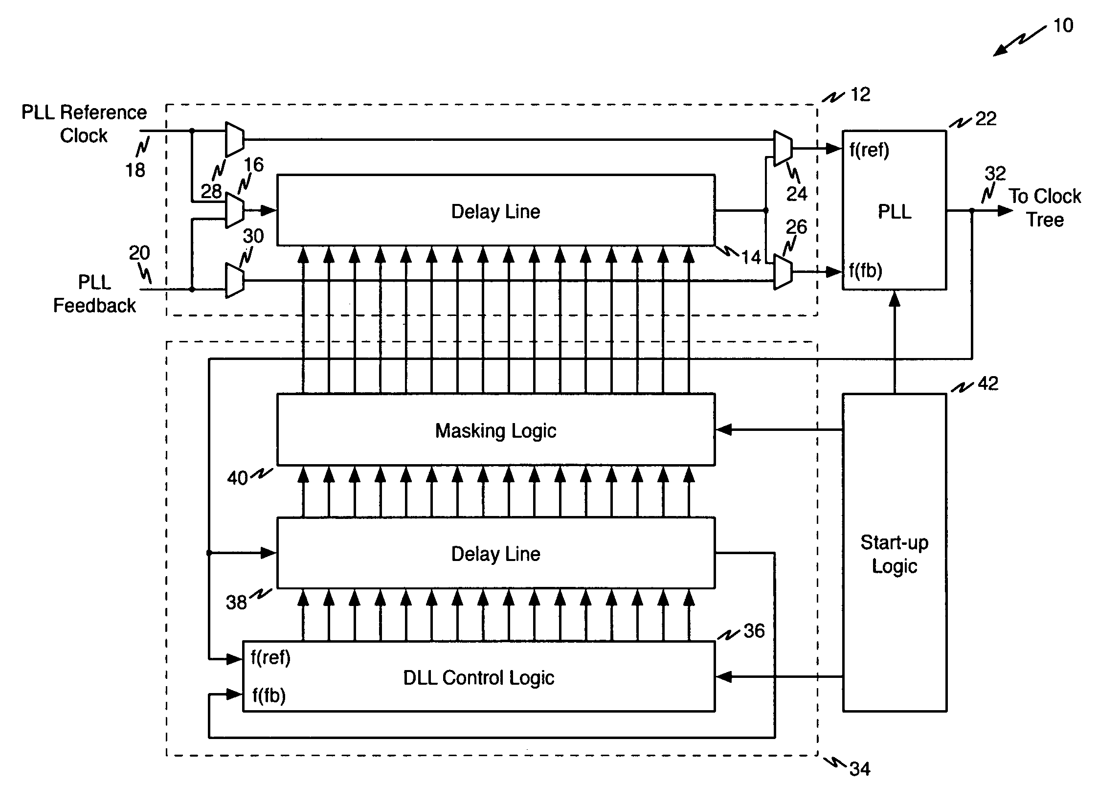
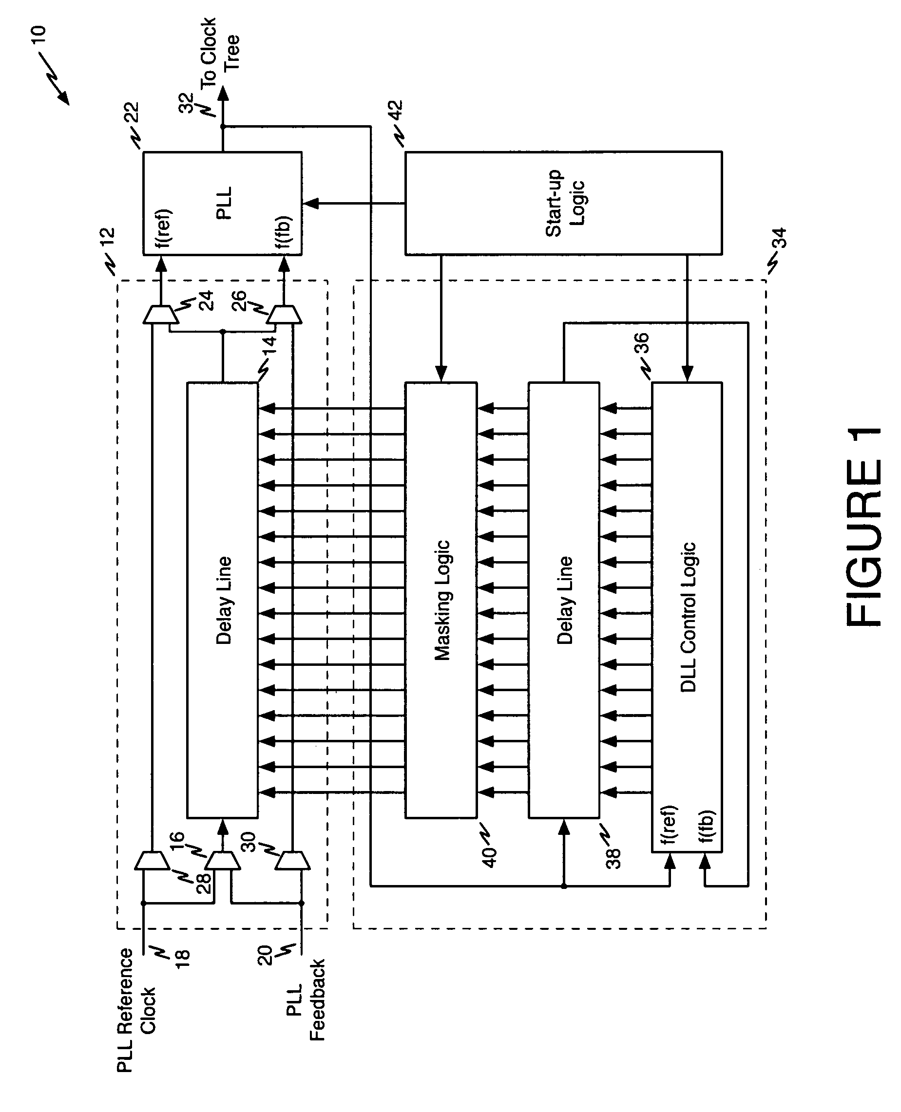
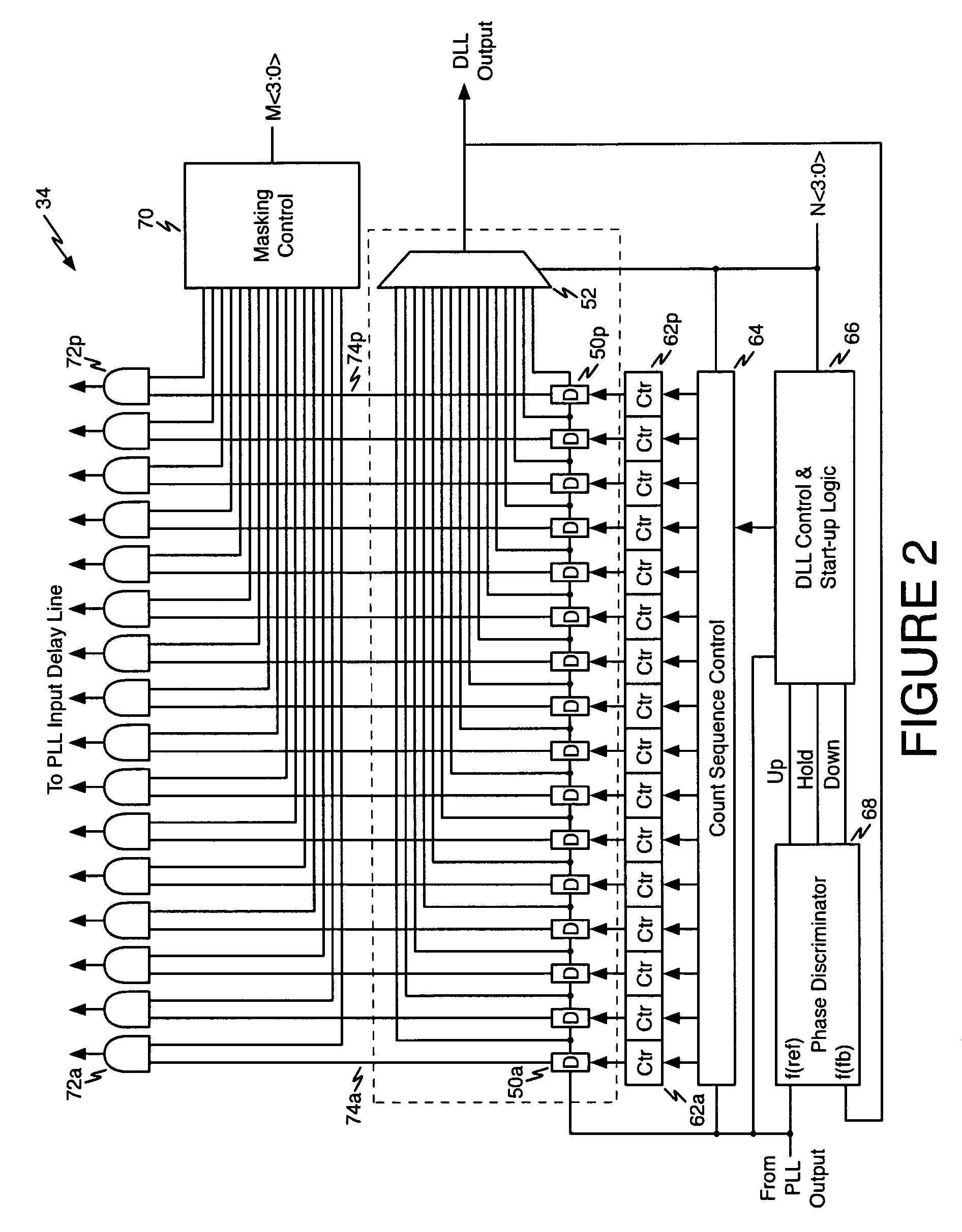
[0030]Referring first to FIG. 1, a block diagram shows an illustrative delay line 10 compensated for process, voltage, and temperature according to the present invention. A PVT-compensated delay line 12 includes a delay line 14. The input to delay line 14 is driven by multiplexer 16 that selectively provides the PLL reference clock on line 18 or the PLL feedback on line 20 to the delay line input.

[0031]The output of delay line 14 is provided to phase-locked loop (PLL) 22 through multiplexers 24 a...


PUM


Abstract

A delay line compensated for process, voltage, and temperature variations, includes a delay locked loop (DLL) configured to delay a digital signal by the clock period of the digital signal, the DLL including a DLL delay line arranged as a plurality of cascaded sub-delay lines each sub-delay line providing one of a plurality of delay quanta in response to a digital control signal. A fractionating circuit is configured to generate a digital delay line control signal that is a fraction of the digital control signal. A digital delay line is arranged as a plurality of cascaded sub-delay lines each sub-delay line providing one of a plurality of delay quanta in response to the digital delay line control signal.

Description

BACKGROUND OF THE INVENTION[0001]1. Field of the Invention[0002]The present invention relates to integrated circuit technology. More particularly, the present invention relates to programmable delay lines compensated for process, voltage, and temperature (PVT).[0003]2. The Prior Art[0004]Non-PVT compensated programmable delays are known in the art. Their use frequently results in delays that are not predictable and are thus often quite different from the ideally desired value.[0005]PVT compensated programmable delay lines are also known in the art like, for example, U.S. Pat. No. 6,958,634 (the '634 patent) issued to Rashid. The '634 patent teaches a master analog delay-locked loop (DLL) establishing a coarse time delay unit governed by analog signals generated from a phase discriminator / charge pump / bias generator arrangement. The analog signals are then used to control a slave delay line comprised of the coarse time delay units. Multiplexers select outputs from adjacent coarse time...

Claims


Application Information

Patent Timeline
Patent Type & Authority Patents(United States)
IPC IPC(8): G06F7/38H03K19/173
CPCH03K5/131H03L7/10H03L7/07H03L7/0805H03L7/0814H03K2005/00123H03K2005/0013H03K2005/00143H03K2005/00156H03L7/0816H03L7/104
Inventor PLANTS, WILLIAM C.ZAIN, SUHAILLANDRY, JOELBAKKER, GREGORY W.JASIONOWSKI, TOMEK
Owner MICROSEMI SOC
Why Eureka
Try Eureka