Semiconductor integrated circuit

a technology of integrated circuits and semiconductors, applied in the direction of power consumption reduction, pulse techniques, instruments, etc., can solve the problems of distortion or bending of current/voltage characteristics of transistors, the inability to ignore characteristic variations, and the kink phenomenon of current/voltage characteristics, etc., to achieve the effect of improving the high-speed operation of circuits and low power consumption

Inactive Publication Date: 2010-05-11
RENESAS ELECTRONICS CORP
View PDF7 Cites 22 Cited by
  • Summary
  • Abstract
  • Description
  • Claims
  • Application Information

AI Technical Summary

Benefits of technology

[0005]The present invention is to provide a semiconductor integrated circuit easy to carry out a body bias suitable for improving a high-speed operation of a circuit using SOI type MOS transistors and low power consumption thereof according to the function and configuration of the circuit.
[0030]It becomes easy to carry out a body bias suitable for improving a high-speed operation of a circuit using SOI type MOS transistors and low power consumption thereof according to the function and configuration of the circuit.

Problems solved by technology

There may be a case in which even though the high-speed operation is required, then a body potential becomes easy to fluctuate when the body is brought into floating, so that a variation in characteristic due to it cannot be ignored.
However, when the positive holes are stored between a portion just above the body and a layer below a channel, a kink phenomenon that distortion or bending occurs in a transistor's current / voltage characteristic takes place.

Method used


Image

  • Semiconductor integrated circuit
  • Semiconductor integrated circuit
  • Semiconductor integrated circuit

Examples


Embodiment Construction

>

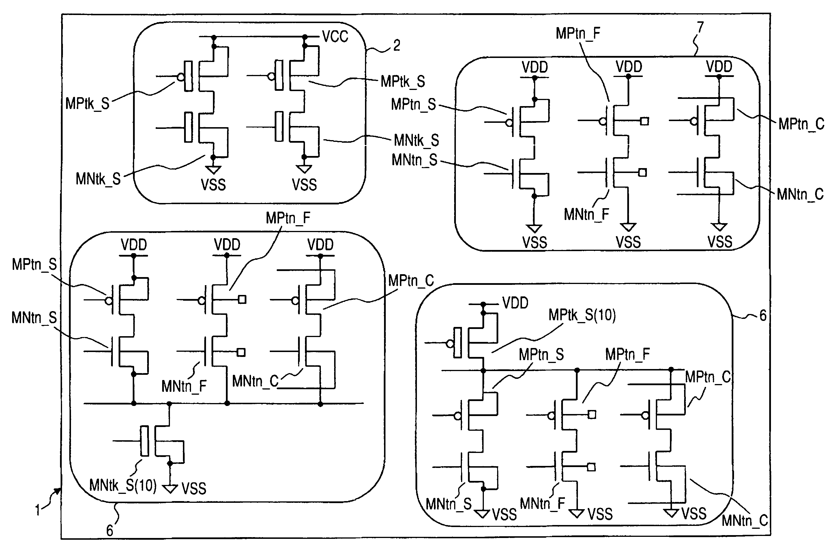
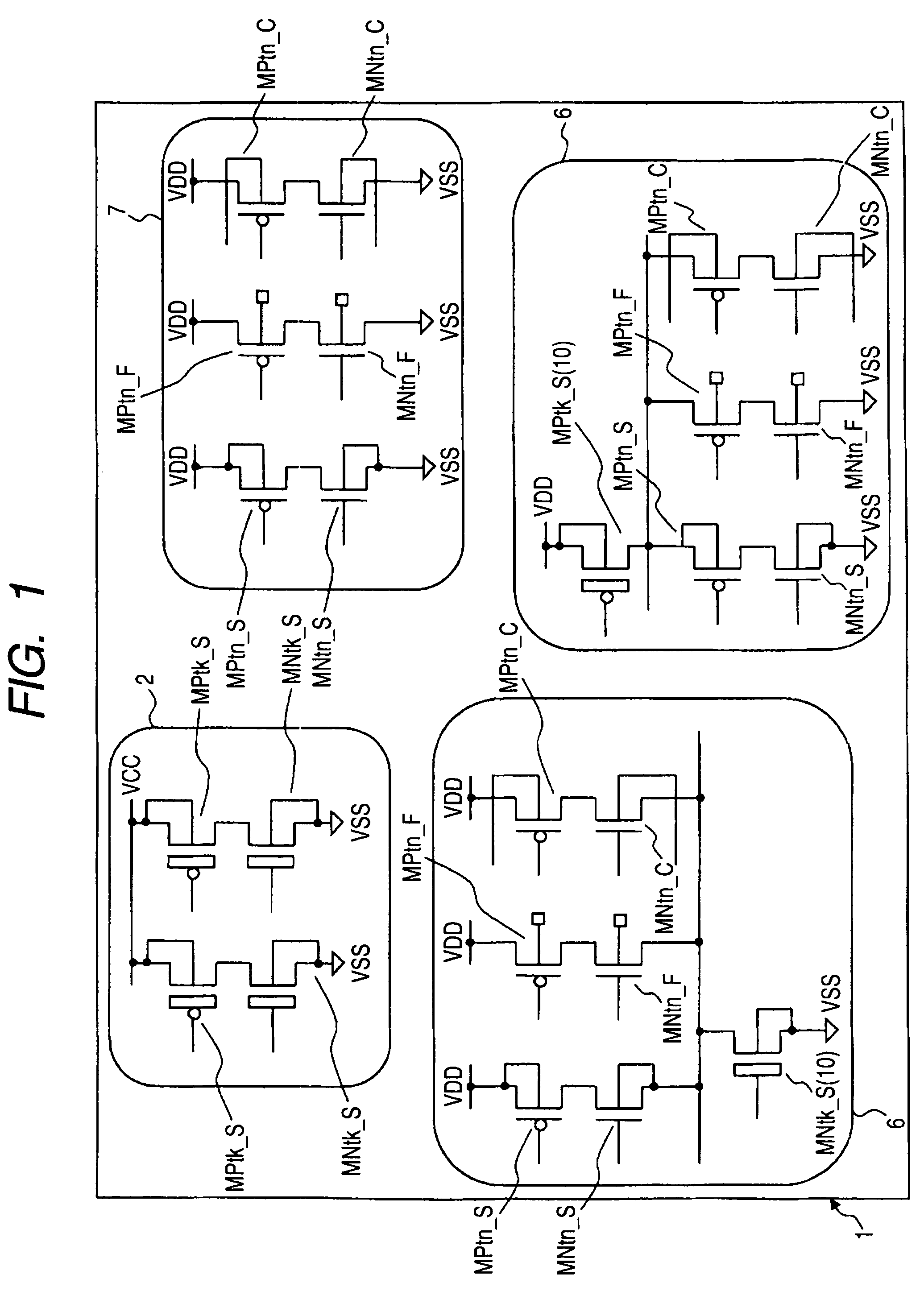
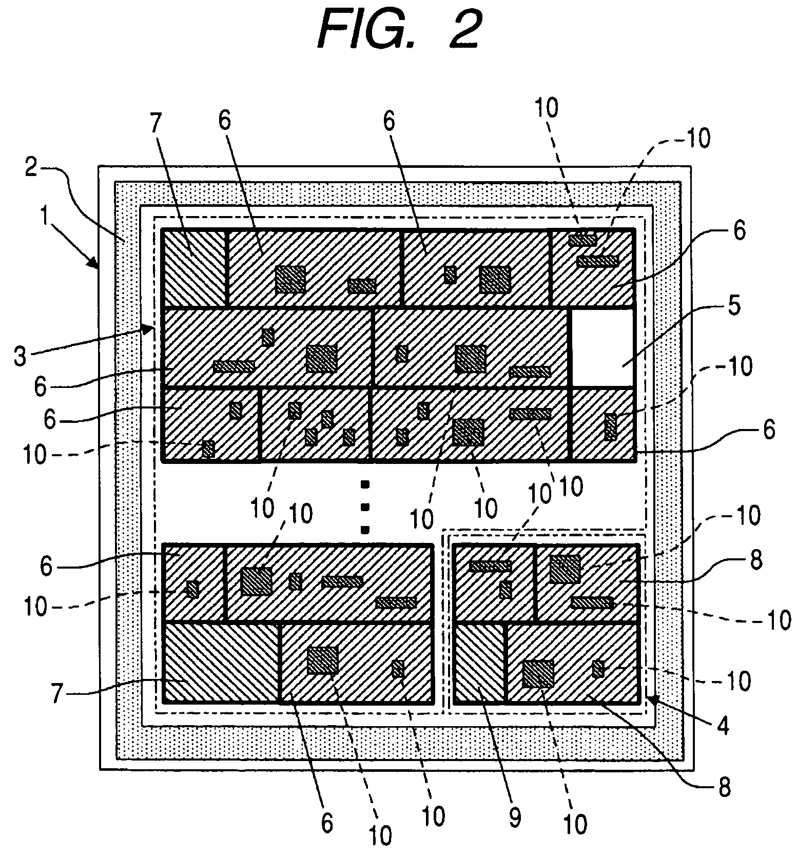
[0084]A planer configuration of a semiconductor integrated circuit 1 according to the present invention is illustrated in FIG. 2. A MOS integrated circuit equipped with a digital / analog-mixed SOI structure is illustrated as one example. A peripheral edge portion of the semiconductor integrated circuit 1 is defined as an area for forming an input / output circuit 2 used as an external interface circuit. A digital circuit area 3 and an analog circuit area 4 are formed inside the area as core circuit areas. A power control and body bias control circuit 5, power shuttable-down circuits 6 each of which makes it possible to selectively shut or block off the supply of operating power by the power control and body bias control circuit 5, and power non-shutdown circuits 7 each of which is always supplied with the applied operating power. The analog circuit area 4 includes power shuttable-down circuits 8 each of which makes it possible to selectively shut off the supply of the operating power ...


PUM


Abstract

A plurality of MOS transistors each having an SOI structure includes, in mixed form, those brought into body floating and whose body voltages are fixed and variably set. When a high-speed operation is expected in a logic circuit in which operating power is relatively a low voltage and a switching operation is principally performed, body floating may be adopted. Body voltage fixing may be adopted in an analog system circuit that essentially dislikes a kink phenomenon of a current-voltage characteristic. Body bias variable control may be adopted in a logic circuit that requires the speedup of operation in an active state and needs low power consumption in a standby state. Providing in mixed form the transistors which are subjected to the body floating and the body voltage fixing and which are variably controlled in body voltage, makes it easier to adopt an accurate body bias according to a circuit function and a circuit configuration in terms of the speedup of operation and the low power consumption.

Description

CROSS-REFERENCE TO RELATED APPLICATION[0001]The present application claims priority from Japanese patent application No. 2006-18876 filed on Jan. 27, 2006, the content of which is hereby incorporated by reference into this application.BACKGROUND OF THE INVENTION[0002]The present invention relates to a semiconductor integrated circuit using SOI (Silicon On Insulator) type field effect transistors (called MOS transistors in the present specification), and particularly to a power shutdown technique thereof.[0003]In a bulk type MOS integrated circuit, active regions are formed in a substrate and well regions to configure MOS transistors. In an SOI type MOS integrated circuit, however, a large number of active regions are formed in an insulating thin film provided on a substrate, without using the well regions, and MOS transistors are configured in the individual active regions. Thus, the SOI type MOS integrated circuit is fundamentally different from the bulk type MOS integrated circuit...

Claims


Application Information

Patent Timeline
Patent Type & Authority Patents(United States)
IPC IPC(8): H03K3/01G05F1/10G05F3/02
CPCH01L27/1203H01L29/7841H03F1/0205H03K19/01707H03K19/0016H03K19/00338H03K19/00384H03F1/301H01L29/78615H03F2200/513
Inventor OZAWA, OSAMUSASAKI, TOSHIOMORI, RYOKURAISHI, TAKASHIYASU, YOSHIHIKO
Owner RENESAS ELECTRONICS CORP
Why Eureka
Try Eureka