High dynamic range imaging cell with electronic shutter extensions

a high-dynamic range, imaging cell technology, applied in the field of image cells, can solve the problems of affecting power and junction leakage, current devices are currently limited in total dynamic range, etc., and achieve the effects of improving the extended dynamic range, low capacitance, and adaptive coupling of a large capacitan

Inactive Publication Date: 2010-05-18
GLOBALFOUNDRIES U S INC
View PDF10 Cites 15 Cited by
  • Summary
  • Abstract
  • Description
  • Claims
  • Application Information

AI Technical Summary

Benefits of technology

[0010]According to the present invention, there is provided a pixel image device having improved extended dynamic range, particularly, by enabling adaptive coupling of a large capacitance via a coupling transistor to the pixel cell when the voltage on the photodiode is drawn down to the substrate potential. Thus, in this manner, the added capacitance is only connected to the imager cell when the cell is nearing its charge capacity. Otherwise, the cell has a low capacitance and low leakage.
[0011]Thus, according to one embodiment of the invention, there is provided a pixel image cell that relies upon the sub-threshold leakage characteristics of a transistor to enable charge carrier leakage into an added capacitor when the voltage on the photodiode is drawn down to the substrate potential. This sub-threshold leakage then continues to fill up the capacitor with its significantly larger (e.g., 2 fF-100 fF) capacitance allowing a 2-50× dynamic range increase.
[0012]Further, there is provided a pixel image cell that exhibits improved dynamic range that relies upon the sub-threshold leakage characteristics of a coupling transistor to leak additional accumulated charge into an added capacitor when the voltage on the photodiode is drawn down to the substrate potential and, that further is equipped with global shutter extensions.

Problems solved by technology

Current devices are currently limited in total dynamic range.
Dynamic range could may increased by utilizing a higher bias voltage, but doing so may negatively impact power and junction leakage.

Method used


Image

  • High dynamic range imaging cell with electronic shutter extensions
  • High dynamic range imaging cell with electronic shutter extensions
  • High dynamic range imaging cell with electronic shutter extensions

Examples


Embodiment Construction

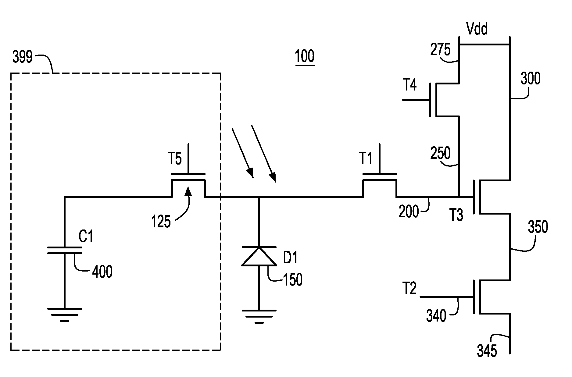
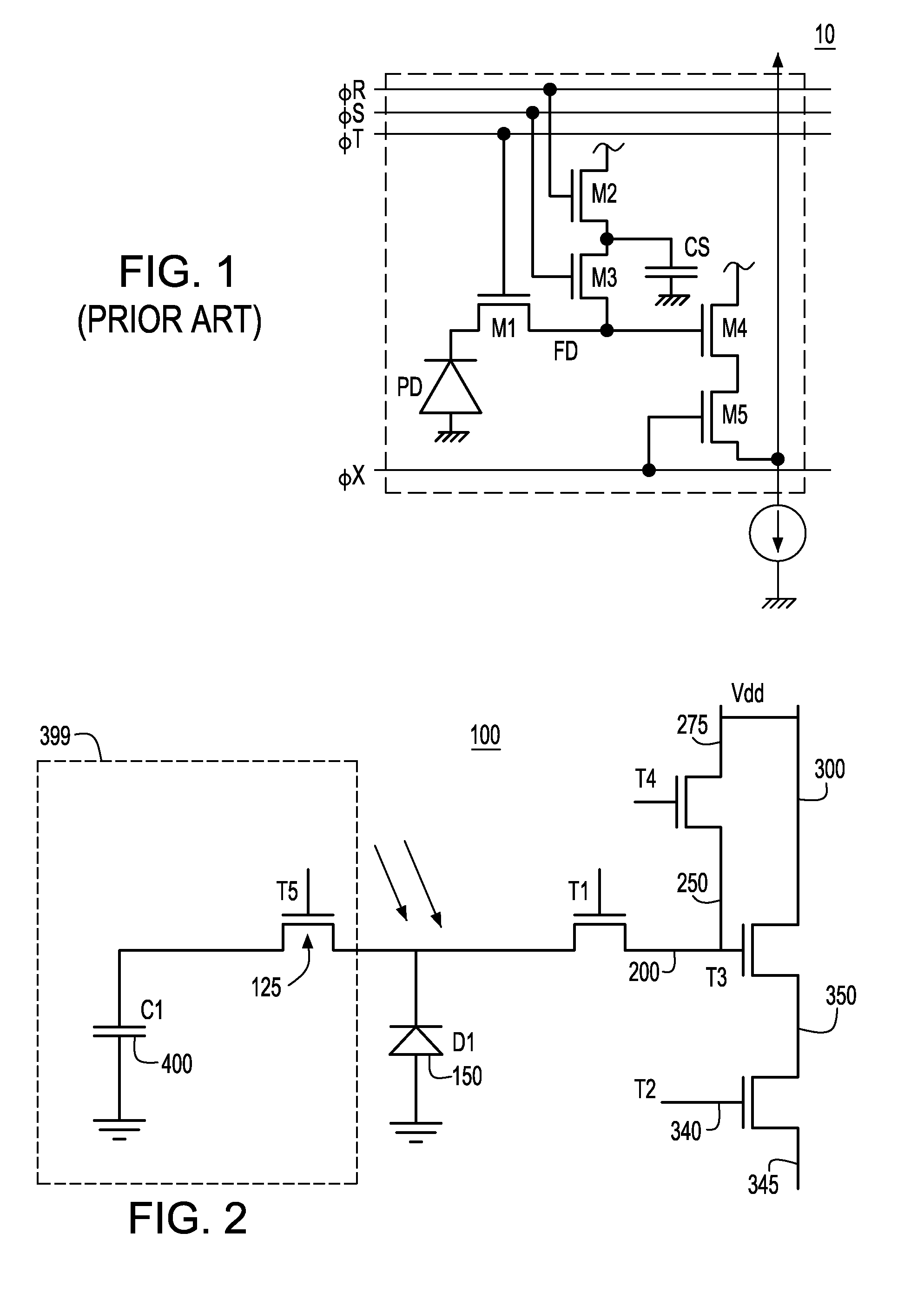
[0031]According to the invention, a new pixel image device is provided that extends dynamic range above and beyond those of conventional image cell devices.

[0032]FIG. 2 depicts the novel pixel cell 100 of the invention that has increased dynamic range as compared to conventional pixel cells. As shown in the circuit of FIG. 2, there is depicted the four (4) device pixel design 100 typically referred to in literature as a 4 device active pixel sensor (APS). The pixel device 100 consists of a first transfer device labeled T1 with a transfer gate, whose one diffusion is the photo diode 150 which collects the incident light, and the other diffusion of the transfer device T1 is referred to as the floating diffusion 200. The floating diffusion 200 is connected to the source 250 of a Reset device T4 having a reset gate, and the drain 275 of the reset device T4 is connected to Vdd which also serves as the reset voltage. Note that sometimes the drain of the reset device is connected to a sepa...


PUM


Abstract

A pixel sensor cell of improved dynamic range comprises a coupling transistor that couples a capacitor device to a photosensing region (e.g., photodiode) of the pixel cell, the photodiode being coupled to a transfer gate and one terminal of the coupling transistor. In operation, the additional capacitance is coupled to the pixel cell photodiode when the voltage on the photodiode is drawn down to the substrate potential. Thus, the added capacitance is only connected to the imager cell when the cell is nearing its charge capacity. Otherwise, the cell has a low capacitance and low leakage. In an additional embodiment, a terminal of the capacitor is coupled to a “pulsed” supply voltage signal that enables substantially full depletion of stored charge from the capacitor to the photosensing region during a read out operation of the pixel sensor cell. In various embodiments, the locations of the added capacitance and photodiode may be interchanged with respect to the coupling transistor. In addition, the added capacitor of the pixel sensor cell allows for a global shutter operation.

Description

FIELD OF THE INVENTION[0001]The present invention relates generally to pixel image sensors, in general, and particularly, an improved image cell having improved dynamic range by use of large capacitance when the cell approaches its charge capacity.DESCRIPTION OF THE PRIOR ART[0002]The requirements for current solid-state image sensors, e.g., CMOS image sensors, are that they be highly sensitive, have a high S / N ratio and a high resolution. However it is desirous to provide pixel image sensor devices with greater dynamic range. Current devices are currently limited in total dynamic range. At the low end devices can not collect less than 1 electron. At the high end, devices are limited to collect up to 30,000 electrons (i.e., approximately 5 fC calculated as 2 fF*2.5V where 2.5 volts is the bias of the sensing photodiode or photosensing device, fF is femptoFarads is the capacitance of the cell and C is coulombs (charge)).[0003]Dynamic range could may increased by utilizing a higher bi...

Claims


Application Information

Patent Timeline
Patent Type & Authority Patents(United States)
IPC IPC(8): H04N5/232
CPCH01L27/14609H04N5/37452H04N5/3559H01L27/14689H01L27/14643H04N25/59H04N25/771
Inventor ELLIS-MONAGHAN, JOHN J.LOISEAU, ALAINPETERSON, KIRK D.
Owner GLOBALFOUNDRIES U S INC
Why Eureka
Try Eureka