Designated MOSFET and driver design to achieve lowest parasitics in discrete circuits

a discrete circuit and driver technology, applied in the field of integrated circuit devices, can solve the problems of insufficient appreciation of pcb layout and circuit parasitics, limited standardized parts, and limited pcb space, so as to minimize circuit vias, avoid a large portion of typical circuit parasitic elements, and minimize circuit vias.

Inactive Publication Date: 2010-05-18
INFINEON TECH AG
View PDF6 Cites 11 Cited by
  • Summary
  • Abstract
  • Description
  • Claims
  • Application Information

AI Technical Summary

Benefits of technology

[0007]The invention relates to an improved MOSFET power stage design for minimizing circuit parasitics, for example, in a DC to DC converter or another such power conversion product, by designating the pin configuration in the package layout of a power MOSFET transistor and MOSFET driver. The present invention makes use of a custom pin configuration for one of the two power MOSFET transistors typically used in the power stage of a power conversion circuit. In one aspect of the invention, the custom pin configuration of the power MOSFET transistor is assigned or designated a complementary package configuration, which is essentially a functional mirror image or a functional complement of an existing pin configuration used in the industry. The complementary package configuration permits a greatly simplified PCB layout design that also minimizes circuit vias, multiple trace segments, and other unnecessary junctions or interconnections to avoid a large portion of the typical circuit parasitic elements.
[0008]Another aspect of the invention relates to a pair of the MOSFET transistors having substantially identical electrical characteristics with complementary package configurations comprising a first and second package and a first and second pin configuration to minimize power stage circuit interconnections and related circuit losses.
[0009]In yet another aspect of the present invention, a MOSFET driver for the transistor pair is also designated a pin configuration associated with a pin configuration of the transistor pair to further minimize the PCB layout and circuit parasitics.
[0011]In one aspect of the present invention, an integral heat sink plate is incorporated into the mounting surface of the MOSFET transistors for thermal conduction to a trace of the PCB. In one implementation, for example, the source of one transistor of the MOSFET transistor pair is electrically connected to the heat sink plate, while the other transistor of the pair connects the drain to the heat sink plate. In this way, the package is able to optimize the circuit layout while minimizing thermal losses.

Problems solved by technology

Although several quasi-standard device footprints have been established for MOSFET transistors, the pool of standardized parts and such alternate or second-sources is limited, particularly in regard to package layouts that are available for higher current devices.
This approach, however, commonly yields an inadequate appreciation of the PCB layout and the circuit parasitics that result from the length / width dimensions of the traces, the capacitance between various circuit elements and traces, or the inductance of circuit vias, for example.
As the trend continues to make MOSFET products smaller and more portable, PCB space becomes scarce and relatively more expensive.

Method used


Image

  • Designated MOSFET and driver design to achieve lowest parasitics in discrete circuits
  • Designated MOSFET and driver design to achieve lowest parasitics in discrete circuits
  • Designated MOSFET and driver design to achieve lowest parasitics in discrete circuits

Examples


Embodiment Construction

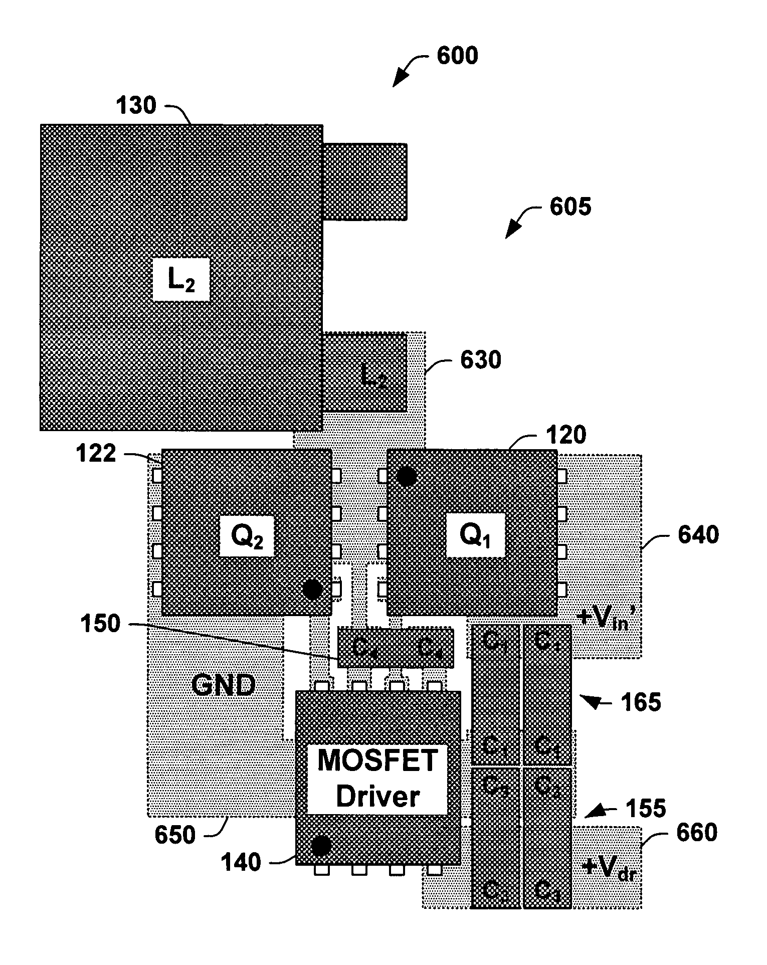
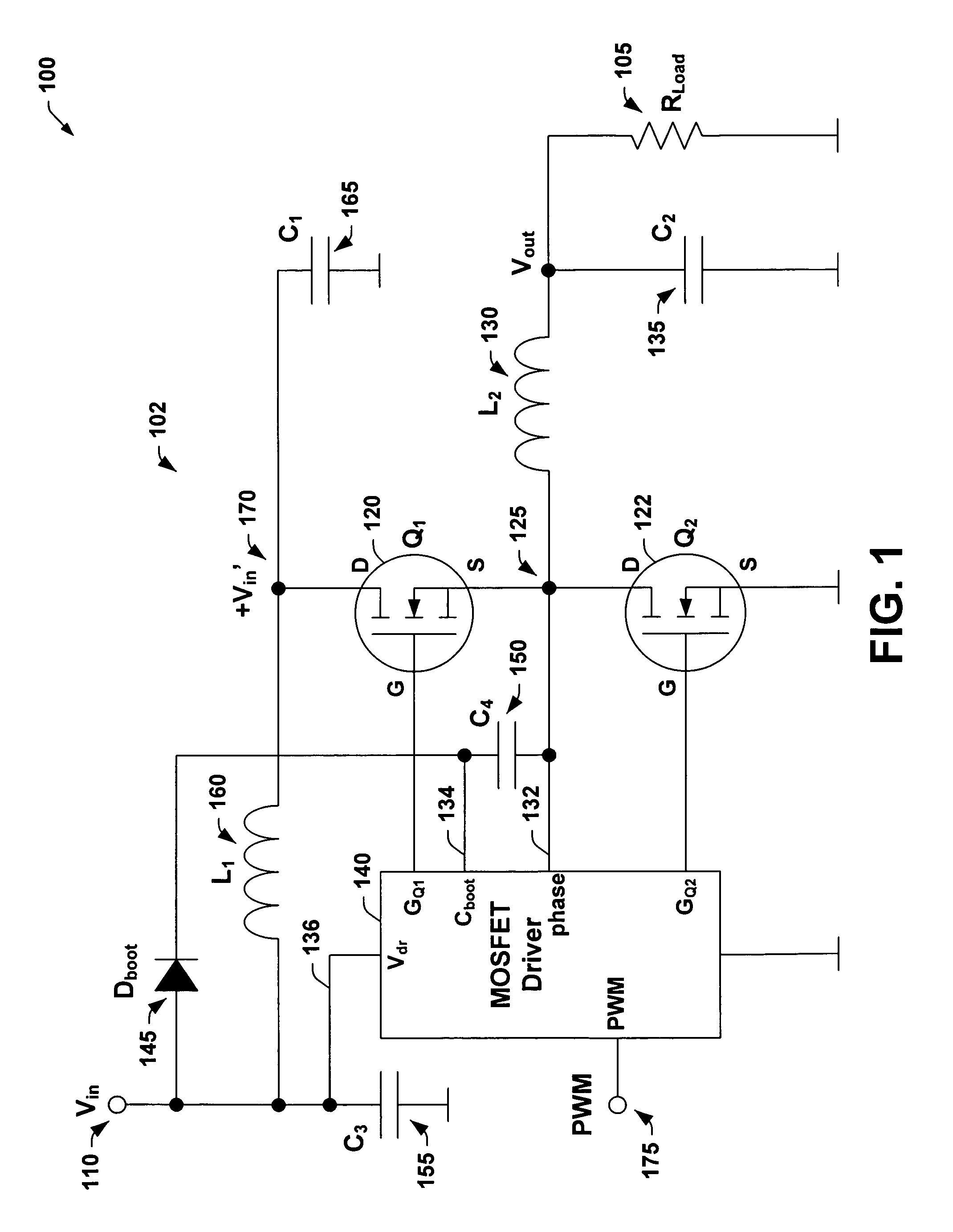
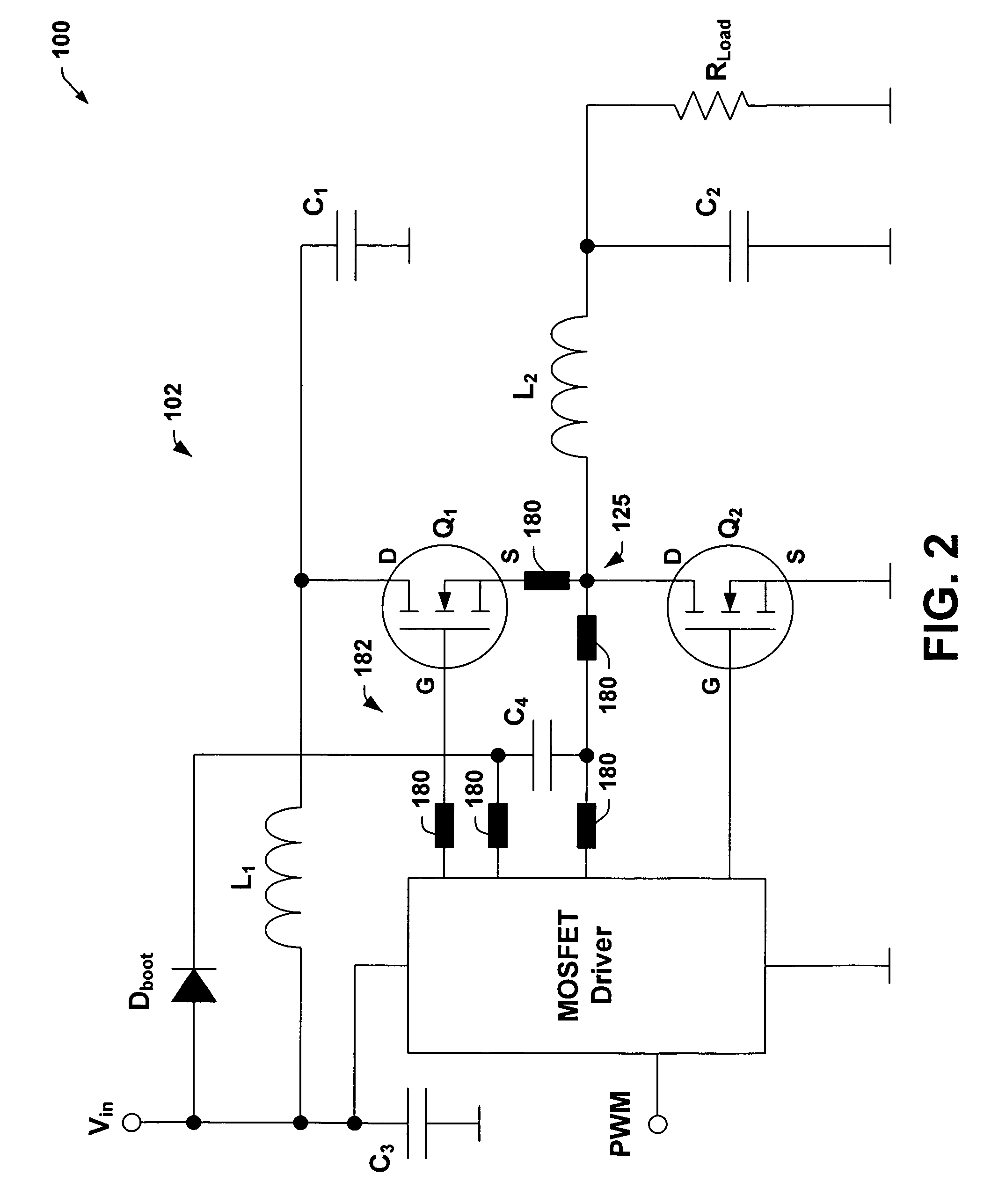
[0021]The present invention will now be described with reference to the attached drawings, wherein like reference numerals are used to refer to like elements throughout. The invention relates to an improved power stage of a MOSFET power conversion product in which the package and pin configuration of a MOSFET power transistor and / or a MOSFET driver is designated to facilitate optimization of a PCB layout in order to avoid or mitigate circuit parasitic elements and their harmful effects.

[0022]Two MOSFET power transistors are often used in the power stage of the MOSFET power conversion device in a push-pull or upper / lower arrangement to provide a symmetrical voltage swing across a load connected to a common circuit node. It has been appreciated by the inventor of the present invention, that because of limited component and second source availability of such transistors particularly in surface mount devices, identical MOSFET transistors are often utilized in a layout requiring less tha...


PUM


Abstract

Apparatus are described for a pair of MOSFET power transistors, a MOSFET driver, and an idealized circuit layout utilized in a power stage such as that of a power conversion system. The power stage comprises a pair of MOSFET transistors having substantially identical electrical characteristics and complementary package configurations for simplifying and optimizing the layout of the power stage on a single side or layer of a printed circuit board. The ideal layout effectively avoids parasitic circuit components, minimizes layout area and costs, and permits operation at higher switching frequencies. A new MOSFET transistor pin configuration is also described that is essentially a functional mirror or functional complement of an existing MOSFET transistor pin configuration to provide the complementary package configurations and the optimized PCB layout. A customized MOSFET driver pin configuration further optimizes the power stage layout by arranging the pins of the driver to coordinate with those of the MOSFET transistor pair.

Description

FIELD OF INVENTION[0001]The present invention relates generally to integrated circuit devices and more particularly to systems and methods for minimizing circuit parasitics in the power stage of a DC to DC converter and other such devices by designating the design of a MOSFET transistor and driver.BACKGROUND OF THE INVENTION[0002]MOSFETs and other types of transistors are found in many modern semiconductor products where switching and / or amplification functions are needed. Speed requirements of MOS transistors continue to increase in order to facilitate higher speed switching frequencies, more phases, and faster transient response for improved product performance. In recent years, the size of MOSFET transistors and other related MOSFET components have only slightly decreased, while available printed circuit board (PCB) space has decreased at a faster pace to facilitate smaller and more portable electronic products. At the same time, many new applications of such devices have created...

Claims


Application Information

Patent Timeline
Patent Type & Authority Patents(United States)
IPC IPC(8): H03F3/38
CPCH01L23/50H02M1/096H02M3/1588H05K1/181H05K1/0203H05K2201/10166H01L2924/0002H05K2201/10522Y02B70/1466H01L2924/00Y02B70/10Y02P70/50H05K1/025
Inventor EJURY, JENS
Owner INFINEON TECH AG
Why Eureka
Try Eureka