Method for measuring information transfer limit in transmission electron microscope, and transmission electron microscope using the same

a technology of transmission electron microscope and information transfer limit, which is applied in the direction of material analysis using wave/particle radiation, instruments, nuclear elements, etc., can solve the problems of substantially restricting the resolution of an electron microscope, the phase of an electron beam cannot be correctly reproduced, and the image formed does not always correctly reflect the structure of an observational entity

Inactive Publication Date: 2010-06-08
HITACHI LTD
View PDF27 Cites 4 Cited by
  • Summary
  • Abstract
  • Description
  • Claims
  • Application Information

AI Technical Summary

Benefits of technology

[0039]FIG. 5A is concerned with a case where a so-called achromatic condition is satisfied and, as mentioned above, the transmitted wave g0 and diffracted wave g1 symmetrically fall on the objective lens 7. Due to the symmetry, the lattice fringes g0(V0−v)+g1(V0−v), lattice fringes g0(V0)+g1(V0), and lattice fringes g0(V0+v)+g1(V0+v) formed at respective energy levels are, as indicated with a boldfaced line in the lower part of FIG. 5A, superimposed on one another while being in phase with one another. Consequently, the amplitude c of the lattice fringes 11 observed as the sum of the lattice fringes in terms of intensities is maximized.
[0055]According to the related art, since the result of measurement largely depends on a specimen, there is difficulty in highly precisely and quantitatively determining an information transfer limit. Further, when a resolution offered by an electron microscope comes to be 0.1 nm or less due to practical use of an aberration correction technology, the conventional measuring method is predicted to reach its limitations. In contrast, according to a measuring method of the present invention, an electron beam produced under a certain condition for diffraction caused by a crystal is used to perform measurement. An information transfer limit of an electron microscope can therefore be estimated highly precisely and quantitatively. Moreover, an information transfer limit of 0.1 nm or less can be measured by appropriately selecting a diffracted wave to be used for measurement. The latter point will be described below by taking a concrete example.

Problems solved by technology

If we observe an entity smaller than the point resolution, the phase of an electron beam cannot be correctly reproduced due mainly to spherical aberration caused by an objective lens.
However, when a specimen is observed using an electron beam that provides a spatial frequency equal to or smaller than the point resolution, since the phase of the electron beam is not correctly reproduced, an image formed does not always correctly reflect the structure of an observational entity.
In this case, a resolution offered by an electron microscope is substantially restricted by the information transfer limit.
Not only the information transfer limit but also an adverse effect such as aberrations caused by a lens, mechanical vibrations, or electromagnetic noise can be discerned.
In reality, even when an amorphous thin film is employed, the image thereof has a specific distribution of spatial frequencies that is not uniform because of the radii of constituent atoms.
There is therefore a high possibility that the information transfer limit dependent on an objective lens may be incorrectly assessed.
Moreover, an internal environment of an electron microscope such as contamination of a specimen largely affects measurement.

Method used


Image

  • Method for measuring information transfer limit in transmission electron microscope, and transmission electron microscope using the same
  • Method for measuring information transfer limit in transmission electron microscope, and transmission electron microscope using the same
  • Method for measuring information transfer limit in transmission electron microscope, and transmission electron microscope using the same

Examples


Embodiment Construction

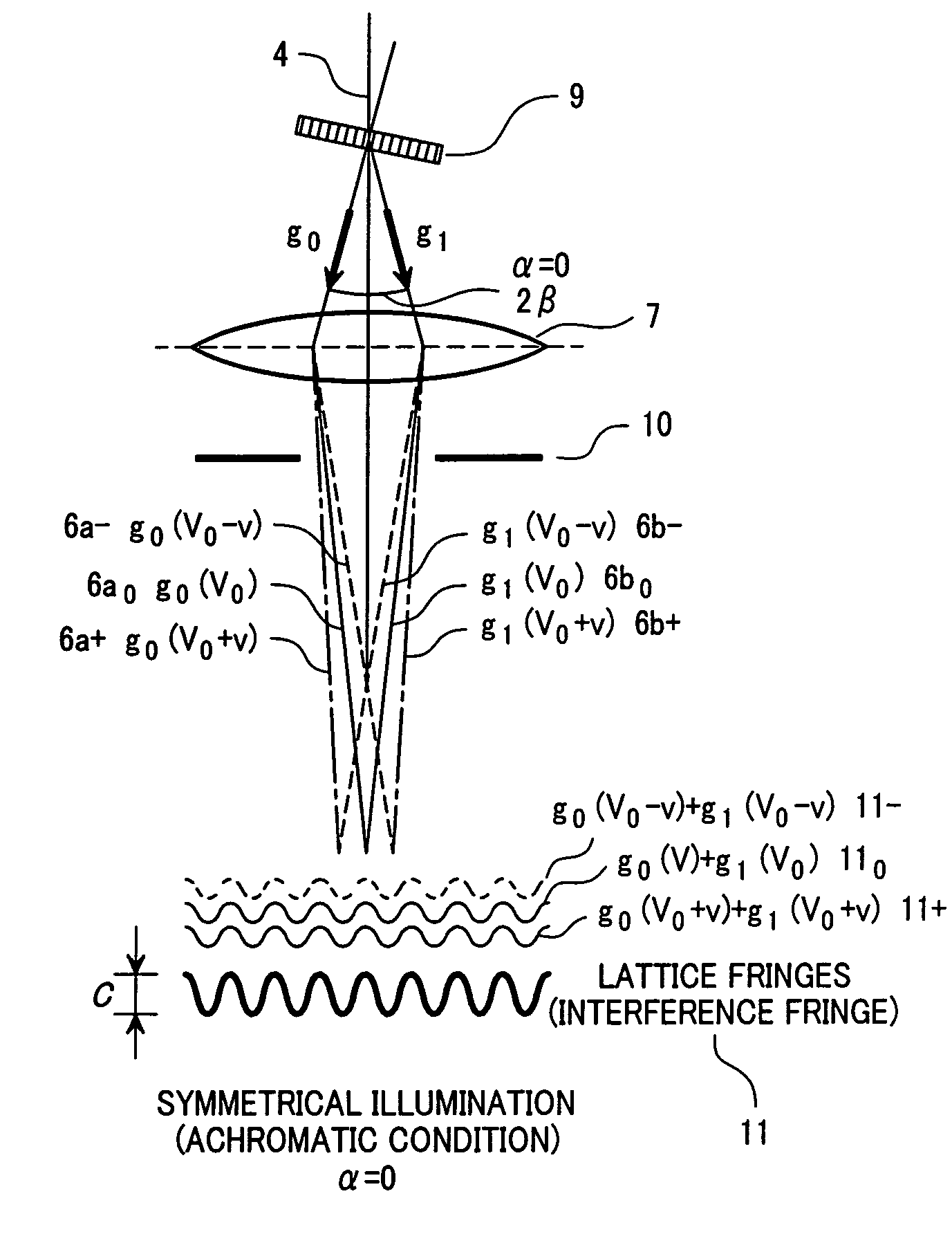
[0064]FIG. 6 illustratively shows the configuration of a transmission electron microscope needed to implement measurement of an information transfer limit in accordance with the present invention. A transmission electron microscope 17 has an electron beam deflector 12 disposed above a crystal thin film 9 for the purpose of changing an incident angle at which an electron beam 4 emanating from an electron source 30 falls on the crystal thin film. Moreover, the transmission electron microscope includes a specimen tilting system 13 that adjusts the angle of a crystalline specimen itself. The electron beam 4 is scattered by the crystal thin film 9, and falls on an objective lens 7 as a diffracted electron beam 6. An aperture system 10 located below the objective lens 7 selects a diffracted wave. A lattice image is formed on an image plane 8 of the objective lens as a result of interference of the selected diffracted wave with other wave. The lattice image is enlarged by intermediate proj...


PUM

PropertyMeasurementUnit
defocus length dfaaaaaaaaaa

Abstract

A crystal thin film is adopted as a specimen for measurement. A change in the contrast of crystal lattice fringes is measured under a condition that a diffracted wave and other wave are caused to interfere with each other. Thus, an information transfer limit of a transmission electron microscope can be measured quantitatively. Since the measurement is performed with a condition for interference restricted, the information transfer limit of the transmission electron microscope can be quantitatively assessed.

Description

CLAIM OF PRIORITY[0001]The present invention claims priority from Japanese application JP 2006-294907, filed on Oct. 30, 2006, the content of which is hereby incorporated by reference on to this application.BACKGROUND OF THE INVENTION[0002](1) Field of the Invention[0003]The present invention relates to a technique for assessing the performance of a transmission electron microscope or a method for measuring an information transfer limit that is a major factor for determining a spatial resolution offered by an electron microscope, and a transmission electron microscope to which the measuring method is adapted.[0004](2) Description of the Related Art[0005]In transmission electron microscopes, a resolution is the most important index of performance. The resolution falls into multiple different definitions such as a point resolution, a lattice resolution, and an information transfer limit that are conventionally used for different purposes.[0006]Among the definitions, the point resoluti...

Claims


Application Information

Patent Timeline
Patent Type & Authority Patents(United States)
IPC IPC(8): G01N23/00G21K7/00
CPCH01J37/263H01J37/28H01J2237/2823H01J2237/2802
Inventor YOSHIDA, TAKAHO
Owner HITACHI LTD
Why Eureka
Try Eureka