Semiconductor device and semiconductor chips outputting a data strobe signal

a technology of semiconductor chips and strobe signals, which is applied in the direction of information storage, static storage, digital storage, etc., can solve the problems of increasing the current of the semiconductor device and unstable operation of the dqs signal level

Active Publication Date: 2010-06-29
LONGITUDE LICENSING LTD
View PDF11 Cites 9 Cited by
  • Summary
  • Abstract
  • Description
  • Claims
  • Application Information

AI Technical Summary

Benefits of technology

[0011]The semiconductor device described in Patent Document 1 is applied to prevent collision between the DQS signals when the DQS signals are output from the DQS terminals of a plurality of the semiconductor chips at the same timing. Such semiconductor device as described above is effective only in case where data outputs from a plurality of the semiconductor chips are separated. Specifically, the semiconductor device as described above is effective in case where semiconductor chips that are different in a word width direction are connected.
[0015]Accordingly, it is an object of the present invention to provide a semiconductor device and semiconductor chips that operate at high speed, without causing increase in a circuit current and unstable operation of a data strobe signal level due to collision between data strobe signals.
[0026]According to the present invention, it is determined whether or not other semiconductor chip is in a read state. When it is determined that the other semiconductor chip is in the read state, an output operation of the data strobe signal is delayed. By this delay, data of opposite levels are not simultaneously output to data strobe signal output drivers of the chips. Accordingly, increase in a circuit current and an unstable operation of a data strobe signal level due to collision between the data strobe signals will not be caused. A high-speed operation can be thereby performed.

Problems solved by technology

For this reason, the DQS signals of opposite polarities are output simultaneously, and may cause an increase in a current of the semiconductor device and an unstable operation of a DQS signal level due to collision between the DQS signals.

Method used


Image

  • Semiconductor device and semiconductor chips outputting a data strobe signal
  • Semiconductor device and semiconductor chips outputting a data strobe signal
  • Semiconductor device and semiconductor chips outputting a data strobe signal

Examples


first example

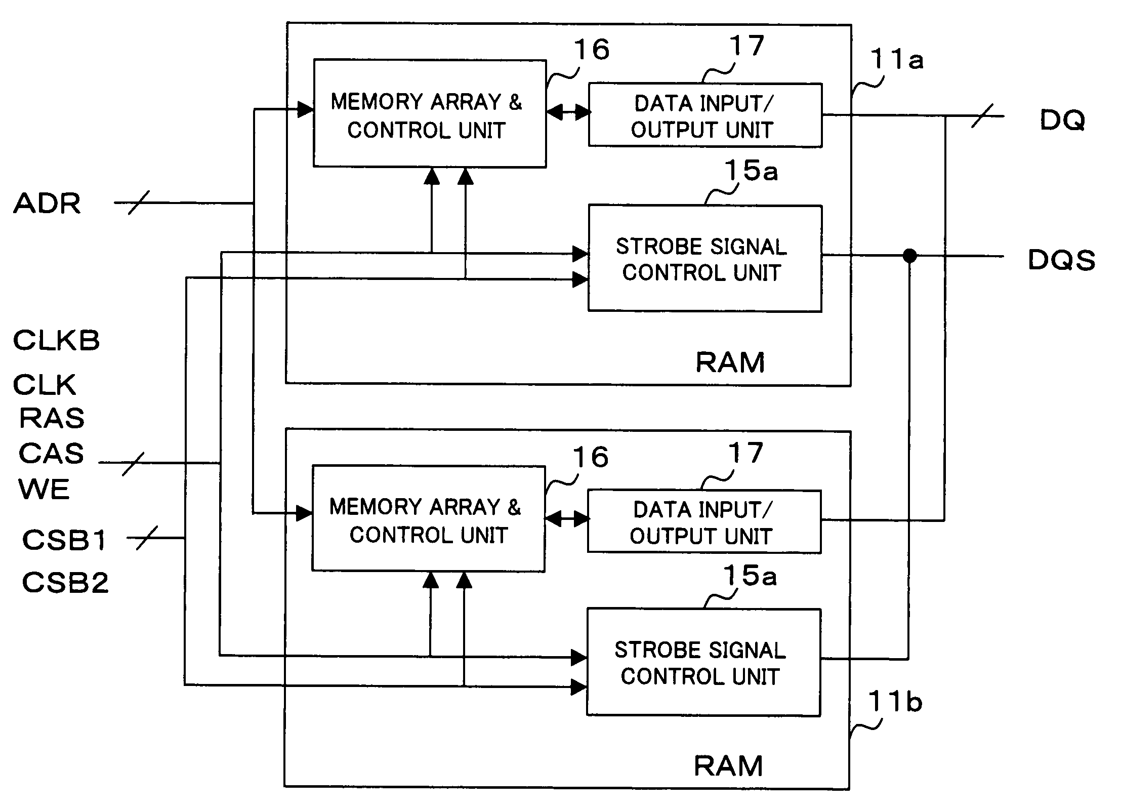
[0044]FIGS. 1A and 1B are block diagrams each showing a configuration of a semiconductor device according to a first example of the present invention. Referring to FIG. 1B, the semiconductor device includes RAMs 11a and 11b on a substrate 10a. The RAMs 11a and 11b are DDR SDRAMs or like having the same configuration as shown in FIG. 1A, and each of the RAMs 11a and 11b includes the strobe signal control unit 15a, a memory array & control unit 16, and a data input / output unit 17. Further, in the RAMs 11a and 11b, wiring for various signals is performed in common by bonding wires from the substrate 10a, as shown in FIG. 1B. Only wirings related to chip select signals CSB1 and CSB2 are formulated so that wiring positions of the signals CSB1 and CSB2 are transposed with each other between RAM 11a and RAM 11b.

[0045]The memory array & control unit 16 is a main unit of each of the RAM 11a and 11b, and operates on clock signals CLK and CLKB, command input signals RAS, CAS, and WE, and the ...

second example

[0070]FIGS. 10A and 10B are block diagrams each showing a configuration of a semiconductor device according to a second example of the present invention. Referring to FIGS. 10A and 10B, same reference numerals as those in FIGS. 1A and 1B indicate same components, and descriptions of the same components will be omitted. The semiconductor device shown in FIGS. 10A and 10B includes RAMs 12a and 12b on the substrate 10b. Each of the RAMs 12a and 12b is the DDR SDRRAM having the same configuration as that as shown in FIG. 10A, and includes a strobe signal control unit 15b, the memory array & control unit 16, and the data input / output unit 17. As shown in FIG. 10B, to the RAMs 12a and 12b, wirings for various signals are routed in common from the substrate 10b by bonding wires, respectively. The chip select signal CSB1 is given as a chip select signal CSB for the RAM 12a. The chip select signal CSB2 is given as the chip select signal CSB for the RAM 12a. Wiring of the chip select signal C...

third example

[0073]FIGS. 12A and 12B are block diagrams each showing a configuration of a semiconductor device according to a third example of the present invention. Referring to FIGS. 12A and 12B, same reference numerals as those in FIGS. 1A and 1B indicate same components, and descriptions of the same components will be omitted. The semiconductor device shown in FIGS. 12A and 12B includes RAMs 13a and 13b on a substrate 10c. Each of the RAMs 13a and 13b is the DDR SDRAM having the same configuration as that as shown in FIG. 12A, and includes a strobe signal control unit 15c, the memory array & control unit 16, and the data input / output unit 17. As shown in FIG. 12B, for the RAMs 13a and 13b, wirings for various signals are routed in common from the substrate 10c by bonding wires, respectively. The chip select signal CSB1 is given as the chip select signal CSB for the RAM 13a. The chip select signal CSB2 is given as the chip select signal CSB for the RAM 13b. Wiring of the chip select signal CS...


PUM


Abstract

High-speed operation is achieved without increase in a circuit current and unstable operation of data strobe signal level due to collision between data strobe signals. Each of RAMs 11a and 11b outputs a data signal DQ and a data strobe signal DQS indicative of an output timing of the data signal. RAM 11a includes a strobe signal control unit 15a that determines whether RAM 11b connected in parallel with the RAM 11a is in a read state or not, and delays an output start timing of data strobe signal DQS when the RAM 11b is in the read state. Strobe signal control unit 15a of the RAM 11a controls output start timing so that a latter half portion of a preamble period of the data strobe signal DQS to be output coincides with a postamble period of the data strobe signal DQS output by the RAM 11b.

Description

REFERENCE TO RELATED APPLICATION[0001]The present application is claiming the priority of the earlier Japanese patent application No. 2006-315746 filed on Nov. 22, 2006, the entire disclosure thereof being incorporated herein by reference thereto.FIELD OF THE INVENTION[0002]The present invention relates to a semiconductor device and semiconductor chips. More specifically, the invention relates to a semiconductor device that includes a plurality of semiconductor chips and outputs a data signal and a data strobe signal indicative of an output timing of the data signal from the semiconductor chips, and the semiconductor chips in such semiconductor device.BACKGROUND OF THE INVENTION[0003]A DDR SDRAM (Double Data Rate Synchronous Dynamic Random Access Memory) is an SDRAM having a high-speed data transfer function capable of performing data reading and writing at both times of a rise and a fall of a clock signal (pulse) for achieving synchronization between circuits. The DDR SDRAM uses a ...

Claims


Application Information

Patent Timeline
Patent Type & Authority Patents(United States)
IPC IPC(8): G11C7/00
CPCG11C7/1027G11C7/1066G11C11/4076G11C7/22G11C7/1072
Inventor INABA, HIDEO
Owner LONGITUDE LICENSING LTD
Why Eureka
Try Eureka