Light emitting device using three-dimensional photonic crystal

a three-dimensional photonic crystal and light-emitting device technology, applied in the direction of optical elements, semiconductor lasers, instruments, etc., can solve the problems of carrier overflow, loss that reduces an internal efficiency, and all the injected carriers do not necessarily contribute to a desired luminescence, etc., to achieve high efficiency and stability

Inactive Publication Date: 2010-07-20
CANON KK
View PDF5 Cites 2 Cited by
  • Summary
  • Abstract
  • Description
  • Claims
  • Application Information

AI Technical Summary

Benefits of technology

[0008]The present invention provides a light emitting device with high efficiency and stability using a three-dimensional photonic crystal.

Problems solved by technology

However, all of the injected carriers do not necessarily contribute to a desired luminescence.
These recombinations cause a loss that reduces an internal efficiency.
As a result, the carrier overflow occurs because of the temperature rise in the active part, and the decrease in internal efficiency is caused.
Since the optical characteristic of the resonator changes if the temperature change occurs in the active part, it is undesirable to cause the temperature change from this respect.
However, the reflected light from the waveguide where the mirror is arranged returns to the resonator to cause a noise.

Method used


Image

  • Light emitting device using three-dimensional photonic crystal
  • Light emitting device using three-dimensional photonic crystal
  • Light emitting device using three-dimensional photonic crystal

Examples


embodiment 1

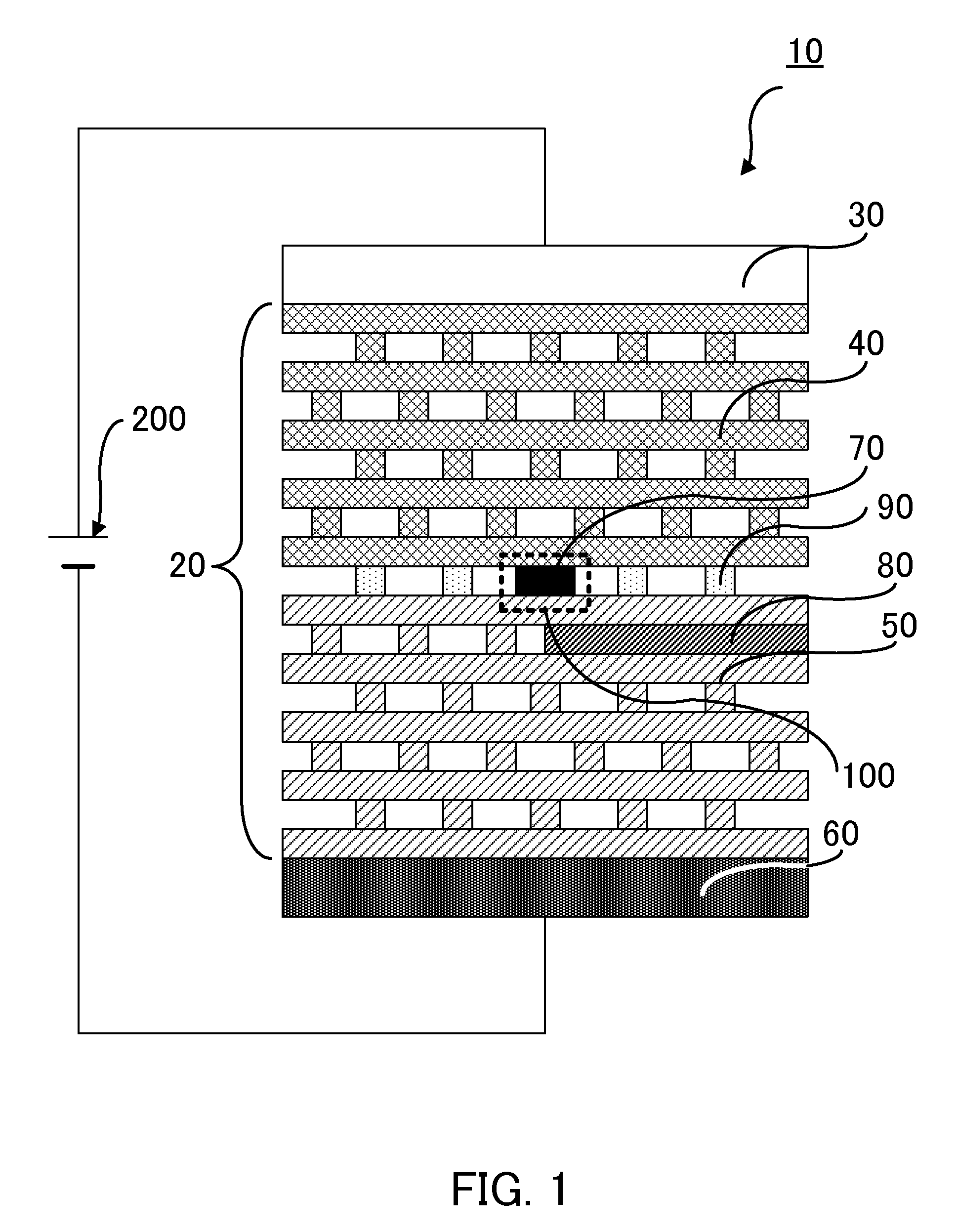
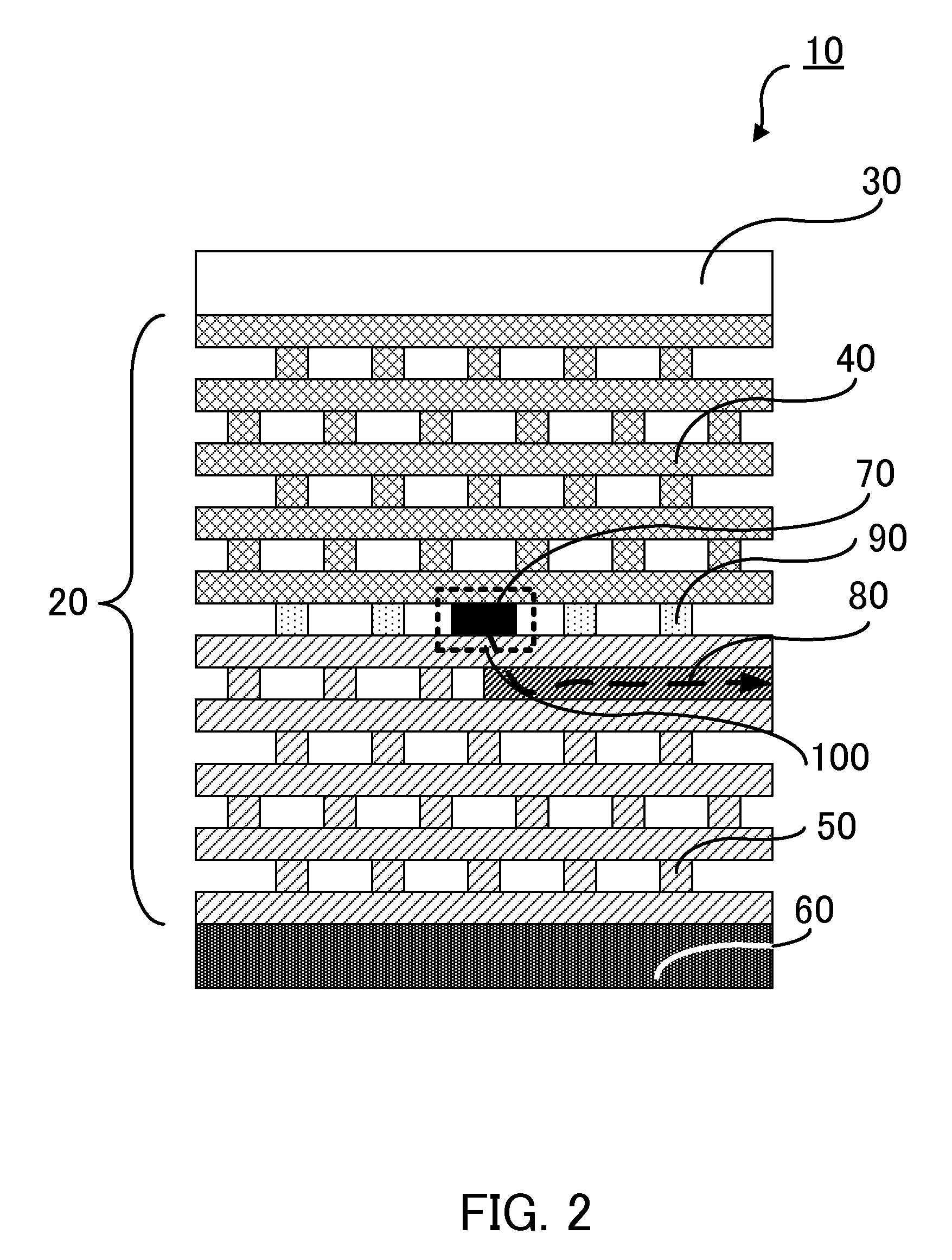
[0021]FIG. 1 shows a cross section of a light emitting device that is embodiment 1 of the present invention. The light emitting device 10 includes a three-dimensional photonic crystal 20, a P-type electrode 30, and an N-type electrode 60. The three-dimensional photonic crystal 20 includes a P clad part 40 formed by a P-type semiconductor, an N clad part 50 formed of a first N-type semiconductor, and an active part 70 and insulated part 90 provided between the P clad part 40 and the N clad part 50. Furthermore, a resonator 100 and a waveguide 80 are formed in the three-dimensional photonic crystal 20.

[0022]The resonator 100 is provided as a point defect part (a first defect part) in the three-dimensional photonic crystal 20. The active part 70 which is formed by an active medium and performs a light emitting action by the injection of the carriers (hole and electron) is provided in the resonator 100. Light is emitted by the recombination of the hole and the electron injected into the...

embodiment 2

[0044]FIG. 4 shows a cross section of a light emitting device that is embodiment 2 of the present invention. A light emitting device 11 of the present embodiment is different from the light emitting device 10 of embodiment 1 in the following points. With regard to the part that has the same function as that of the light emitting device 10 of embodiment 1, the same numeral as embodiment 1 is denoted and the description thereof is omitted.

[0045]In the light emitting device 11 of the present embodiment, a current constricting area 91 formed of a material that has an electrical conductivity lower than that of the P-type semiconductor, i.e. a material that has an electrical resistance greater than that of the P-type semiconductor, is provided in a part of the P clad part 41. The current constricting area 91 provided in the P clad part 41 can concentrate the holes near the active part 70 and further ease the excess of the electrons and the shortage of the holes in the vicinity of the acti...

embodiment 3

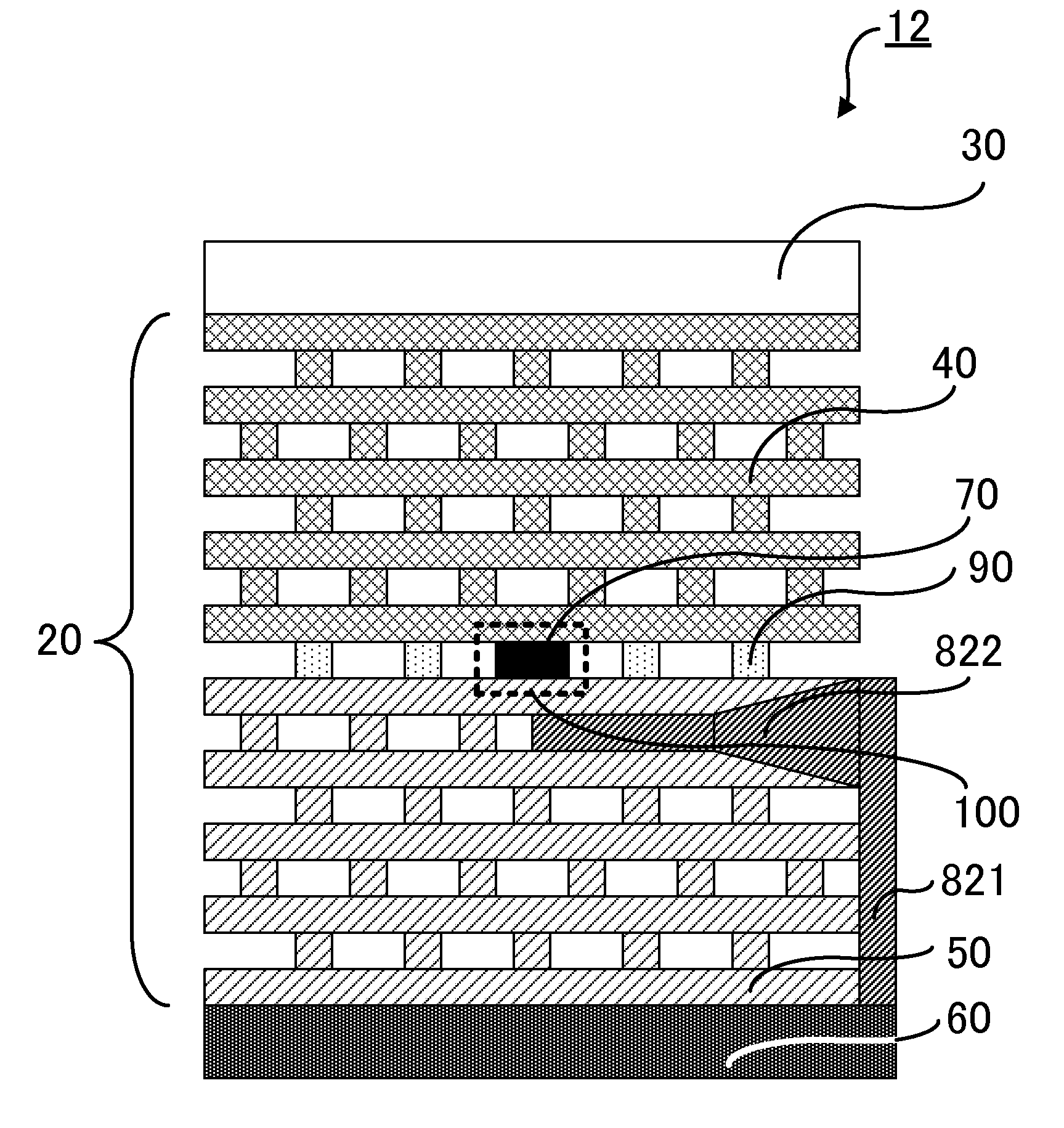
[0048]FIG. 6 shows a cross section of a light emitting device that is embodiment 3 of the present invention. A light emitting device 12 of the present embodiment is different from the light emitting device 10 of embodiment 1 in the following points. With regard to the part that has the same function as that of the light emitting device 10 of embodiment 1, the same numeral as embodiment 1 is denoted and the description thereof is omitted.

[0049]In the light emitting device 12 of the present embodiment, a heat transfer structure 821 formed as a board structure is arranged on an edge surface at an exit side of a waveguide 82 (an exit side edge part). The heat transfer structure 821 is arranged so as to contact the exit side edge part of the waveguide 82 and is also connected to the N-type electrode 60.

[0050]As a result, the heat generated near the active part 70 can be transferred to the N-type electrode 60 through the waveguide 82 and the heat transfer structure 821 to be radiated from...


PUM


Abstract

In a light emitting device, efficiency and stability are improved. A light emitting device 10 includes a three-dimensional photonic crystal 20. The three-dimensional photonic crystal includes a first defect part 70 forming a resonator including an active medium, a second defect part 80 forming a waveguide for taking out light generated by the resonator, a P clad part 40 formed of a P-type semiconductor, and a N clad part 50 formed of a first N-type semiconductor. The second defect part is provided only in the N clad part among the P clad part and the N clad part. At least a part of the second defect part is formed of a second N-type semiconductor and constitutes a heat radiation unit which radiates a heat to the outside.

Description

BACKGROUND OF THE INVENTION[0001]The present invention relates to a light emitting device such as a light emitting diode (LED) or a laser diode (LD) which includes a three-dimensional photonic crystal and emits light by injecting a carrier into an active medium.[0002]A conventional general semiconductor light emitting device has electrodes, clad parts, and an active part. A hole is injected into the active part from a P-type electrode through a P clad part and an electron is injected into the active part from an N-type electrode through an N clad part. Both carriers are recombined in the active part and spontaneous emitted light that has energy corresponding to an energy gap of the active part is emitted. In particular, when a resonator is formed so as to include the active part with a cleaved surface or the like, stimulated emitted light is generated by a light amplification by the resonator to generate a laser beam.[0003]However, all of the injected carriers do not necessarily con...

Claims


Application Information

Patent Timeline
Patent Type & Authority Patents(United States)
IPC IPC(8): G02B6/26G02B6/10G02B6/28
CPCB82Y20/00G02B6/12004G02B6/1225H01L33/16H01S5/10H01L2933/0083H01S5/024H01S5/02461H01S5/0425H01S5/1032H01S5/105H01S5/04253H01S5/04254H01S5/11
Inventor NUMATA, AIHIKO
Owner CANON KK
Why Eureka
Try Eureka