Design method and system for minimizing blind via current loops

a current loop and design method technology, applied in cross-talk/noise/interference reduction, printed circuit aspects, instruments, etc., can solve the problems of increasing design time, complex and computation-intensive accurate models, and unplanned coupling to signal vias, etc., to achieve the effect of reducing the area

Active Publication Date: 2010-07-27
SIEMENS PROD LIFECYCLE MANAGEMENT SOFTWARE INC
View PDF8 Cites 15 Cited by
  • Summary
  • Abstract
  • Description
  • Claims
  • Application Information

AI Technical Summary

Problems solved by technology

Further, if the net lowest impedance return path includes signal vias, undesired coupling to the signal vias will also occur.
Extensive electromagnetic circuit analysis is not typically undertaken for determining such inductive effects and coupling, as accurate models are complex and computation-intensive.
Furthermore, such modeling would have to be performed for each design iteration, dramatically increasing design time.
Existing non-analytic techniques, such as automated or visual inspection of signal paths are typically two-dimensional and therefore do not take into account the three-dimensional nature of the problem.

Method used


Image

  • Design method and system for minimizing blind via current loops
  • Design method and system for minimizing blind via current loops
  • Design method and system for minimizing blind via current loops

Examples


Embodiment Construction

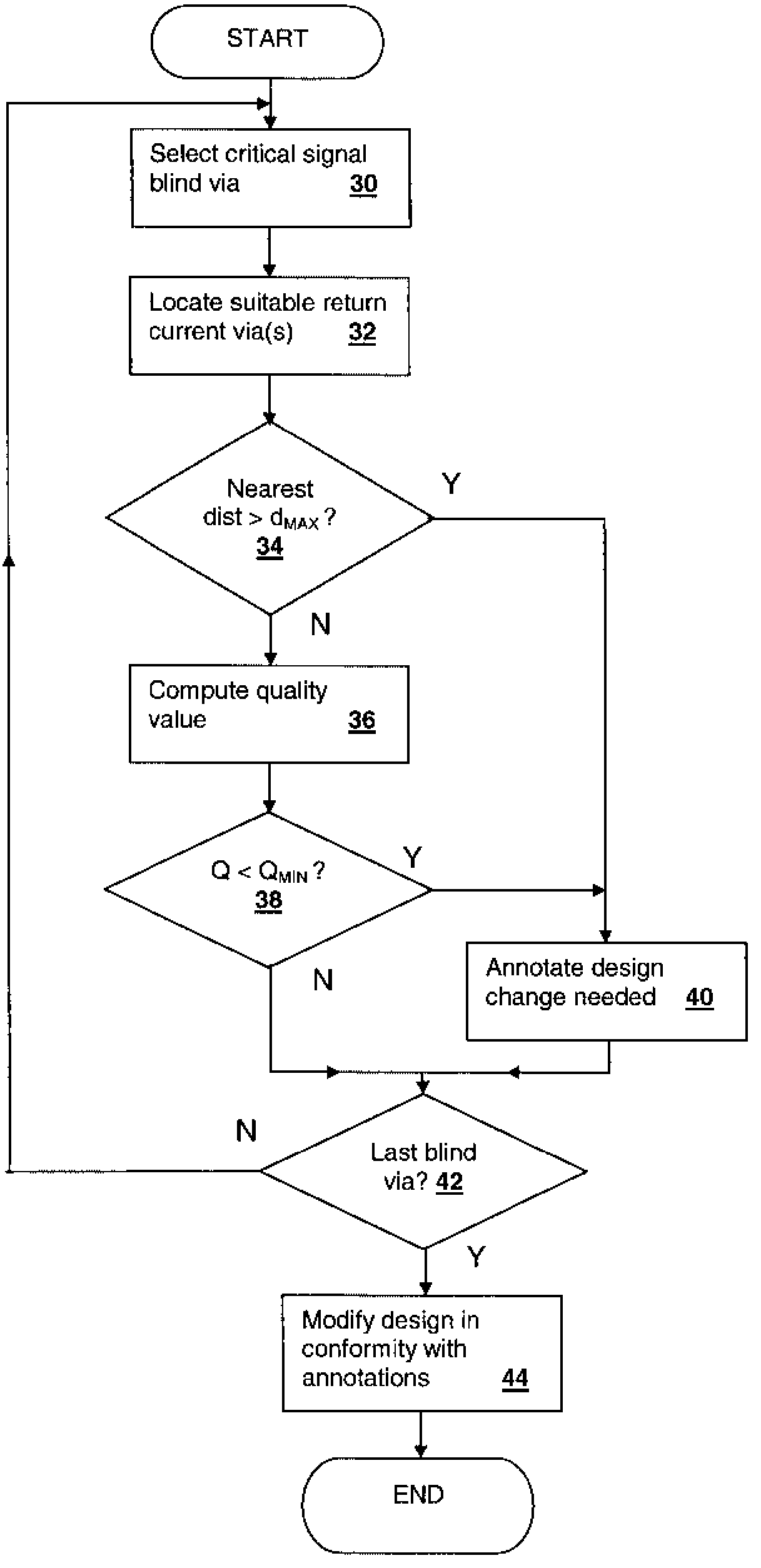
[0017]The present invention concerns design methods and software for designing integrated circuit package substrates such as organic first level interconnect (FLI) packages, and other interconnecting circuit structures such as printed wiring boards (PWB), silicon interposers and any other structures relying on blind vias to provide interconnects for critical signals. The methods and software reduce the electromagnetic impact of discontinuities caused by blind vias carrying critical signals. Electromagnetic analysis is not required in the method or software, as the method provides design checks and design criteria that are imposed on the physical position of blind vias and other vias, in accordance with signal types for each of the vias as denoted in a netlist.

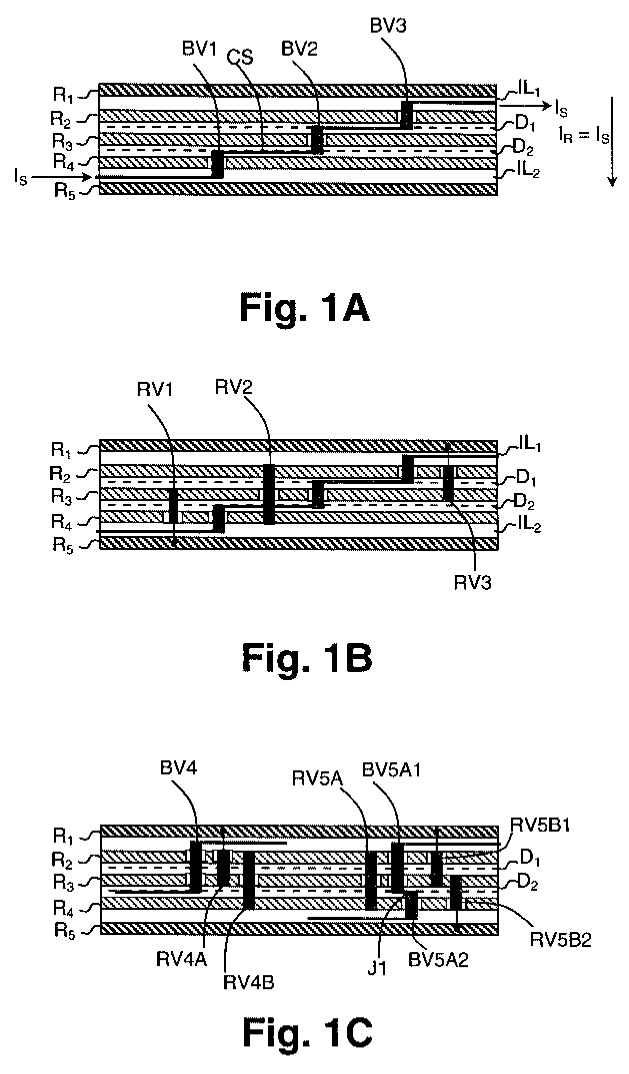
[0018]Referring now to FIG. 1A, a cross-section of an integrated circuit substrate that can be analyzed in accordance with an embodiment of the invention, is shown. A core formed from dielectric layers D1 and D2 sandwiched betw...


PUM


Abstract

A design method and system for minimizing blind via current loops provides for improvement of electrical interconnect structure design without requiring extensive electromagnetic analysis. Other vias in the vicinity of a blind via carrying a critical signal are checked for suitability to conduct return current corresponding to the critical signal that is disrupted by the transition from a layer between two metal planes to another layer. The distance to the return current via(s) is checked and the design is adjusted to reduce the distance if the distance is greater than a specified threshold. If the blind via transition is to an external layer, suitable vias connect the reference plane at the internal end of the blind via to an external terminal. If the transition is between internal layers, suitable vias are vias that connect the two reference planes surrounding the reference plane traversed by the blind via.

Description

BACKGROUND OF THE INVENTION[0001]1. Technical Field[0002]The present invention relates generally to circuit design software, and more particularly, to a methodology and computer program that perform design checks and design modification of buried blind via structures to minimize vertical current discontinuities.[0003]2. Description of the Related Art[0004]High-density interconnect schemes within and between processor packages and other very-large-scale integrated (VLSI) circuits, typically use a large number of circuit layers to connect one or more dies to electrical terminals disposed on one or more surfaces of the package, as well as to interconnect multiple dies in multi-die packages. With the high frequencies and / or narrow pulse widths of critical signals in present-day VLSI circuits, special layout techniques are typically required for routing critical signal paths to minimize reflections, impedance mismatches and coupling between signal paths, according to electromagnetic anal...

Claims


Application Information

Patent Timeline
Patent Type & Authority Patents(United States)
IPC IPC(8): G06F17/50
CPCG06F17/5081H05K3/0005H05K1/0216H05K1/115H05K2201/09636G06F30/398
Inventor DOURIET, DANIELHARIDASS, ANANDHUBER, ANDREASWEEKLY, ROGER D.
Owner SIEMENS PROD LIFECYCLE MANAGEMENT SOFTWARE INC
Why Eureka
Try Eureka