Organic electroluminescent display device and method of fabricating the same

a technology of electroluminescent display device and electroluminescent light, which is applied in the direction of static indicating device, discharge tube luminescnet screen, instruments, etc., can solve the problems of preventing use in large-area displays, low power consumption of electroluminescent display devices, and high brightness, so as to improve surface potential, reduce current, and improve the effect of threshold voltag

Active Publication Date: 2010-08-03
LG DISPLAY CO LTD
View PDF1 Cites 3 Cited by
  • Summary
  • Abstract
  • Description
  • Claims
  • Application Information

AI Technical Summary

Benefits of technology

[0021]An object of the present invention is to provide an organic electroluminescent display device and a method of fabricating the same that improve shift of threshold voltage and decrease current.
[0022]Another object of the present invention is to provide an organic electroluminescent display device and a method of fabricating the same that improve a surface potential between an active layer and a gate insulating.

Problems solved by technology

The organic electroluminescent display device also has a low power consumption, high brightness, and a short response time.
However, the passive matrix-type organic electroluminescent display devices have high power consumption, thereby preventing use in large area displays.
However, the current may decrease due to long term degradation of the driving element.

Method used


Image

  • Organic electroluminescent display device and method of fabricating the same
  • Organic electroluminescent display device and method of fabricating the same
  • Organic electroluminescent display device and method of fabricating the same

Examples


Embodiment Construction

[0039]Reference will now be made in detail to the illustrated embodiment of the present invention, an example of which is illustrated in the accompanying drawings.

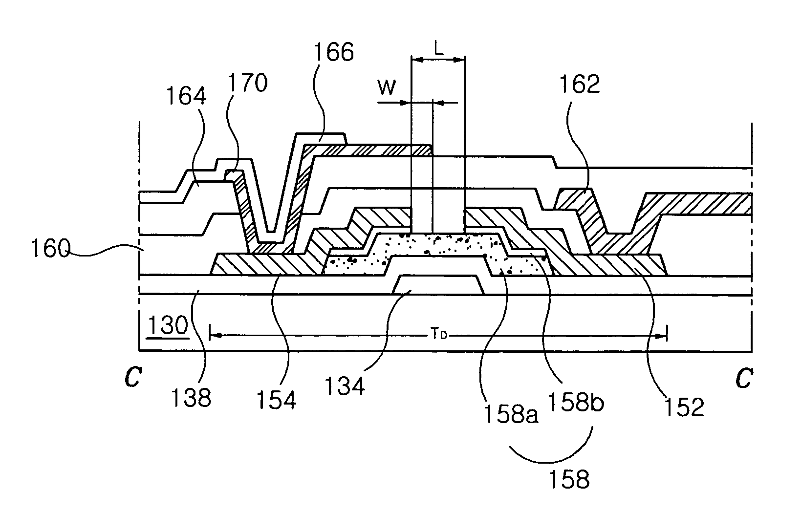
[0040]FIG. 6 is a plan view of an organic electroluminescent display (OELD) device according to an exemplary embodiment of the present invention. FIG. 7 is a cross-sectional view along line C-C of FIG. 6 and illustrates a driving element of the OELD device shown in FIG. 6. FIG. 8 is an equivalent circuit of a pixel for the OELD device shown in FIG. 6. In an embodiment of the present invention, an amorphous silicon thin film transistor may be used as a switching element and a driving element.

[0041]As shown in the figures, a gate line 136 is formed on a substrate 130 along a direction, and a data line 149 crosses the gate line 136 to define a pixel region. A ground line 162 is parallel to the data line 149 crossed the gate line 136.

[0042]A switching element TS is formed at a crossing point of the gate and data lines 136 and ...


PUM


Abstract

An organic electroluminescent display device includes a substrate, gate and data lines on the substrate and crossing each other to define a pixel region, a switching element at each crossing point of the gate and data lines, a driving element coupled to the switching element, a field control electrode coupled to the driving element and overlapping a channel of the driving element, and an organic electroluminescent diode coupled to the driving element.

Description

[0001]The present invention claims the benefit of Korean Patent Application No. 2004-0030092 filed in Korea on Apr. 29, 2004, which is hereby incorporated by reference.BACKGROUND OF THE INVENTION[0002]1. Field of the Invention[0003]The present invention relates to an electroluminescent display device, and more particularly, to an organic electroluminescent display device including thin film transistors with amorphous silicon as active layers and a method of fabricating the same. Although the present invention is suitable for a wide scope of applications, it is particularly suitable for improving shift of threshold voltage and decreasing current in an organic electroluminescent display device.[0004]2. Discussion of the Related Art[0005]In general, an organic electroluminescent display device emits light by injecting electrons from a cathode electrode and holes from an anode electrode into an emissive layer, combining the electrons and the holes to generate an exciton, and by transiti...

Claims


Application Information

Patent Timeline
Patent Type & Authority Patents(United States)
IPC IPC(8): H01L33/00H05B33/00G09G3/32H01J1/62H01J63/04H01L21/77H01L27/12H01L27/32H01L29/786
CPCG09G3/3233H01L29/78648H01L27/1214G09G2300/0417G09G2300/0819G09G2320/043H01L27/3244G09G2300/0842H10K59/12E04G17/0657
Inventor CHUNG, IN-JAEKIM, KI-YONGHAN, CHANG-WOOKHWANG, KWANG-JO
Owner LG DISPLAY CO LTD
Why Eureka
Try Eureka