Plasma processing method and film forming method

a processing method and film technology, applied in the field of plasma processing method and film forming method, can solve the problems of low mechanical strength of such a porous low-k film, film peeling may occur, and low-k film degradation, etc., and achieve the effect of uniform curing

Inactive Publication Date: 2010-08-10
TOKYO ELECTRON LTD
View PDF10 Cites 371 Cited by
  • Summary
  • Abstract
  • Description
  • Claims
  • Application Information

AI Technical Summary

Benefits of technology

[0009]An object of the present invention is to provide a plasma processing method by which, when curing processing is carried out on a Low-k film, the Low-k film can be made to have a reduced dielectric constant, curing can be carried out uniformly through out the entirety of the film, and also, adherence can be improved.
[0016]In the plasma processing method according to the present invention, by controlling a timing of plasma ignition, an influence of Ar ions or such on a low dielectric constant film produced on a to-be-processed substrate can be reduced to the utmost, and thus, uniform curing can be achieved with active hydrogen (such as hydrogen radicals, hydrogen ions or such) without an increase of a dielectric constant of the film.

Problems solved by technology

Generally speaking, mechanical strength of such a porous Low-k film is low, and therefore, film peeling may occur, when copper is embedded and flattening is carried out in CMP after the Low-k film is produced.
When curing processing of a Low-k film is carried out by the above-mentioned thermal processing, UV processing or electronic beam processing, degradation in the Low-k film may occur, such as an increase in a film shrinkage factor or such.
Further, when plasma processing is carried out on a Low-k film in a method such as that described above with reference to FIG. 16, a cured film is produced only in the vicinity of a surface of the Low-k film, and curing may not be carried out inside deeply.
Thus, proper control of an etched shape may become difficult.
Furthermore, when only the vicinity of the surface of the film is cured, the original purpose of curing processing cannot be sufficiently achieved accordingly, a mechanical strength of the Low-k film may not be sufficiently increased, a wall part configuring a wiring pattern may fall down, and thus, a subsequent process may not be carried out.
Further, since wetting property (adherence) may not be sufficient, and thus film peeling may occur, so that leakage electric current may increase.

Method used


Image

  • Plasma processing method and film forming method
  • Plasma processing method and film forming method
  • Plasma processing method and film forming method

Examples


Embodiment Construction

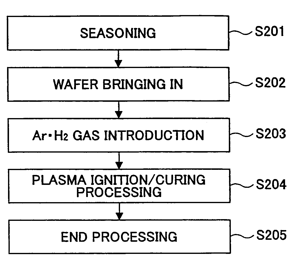
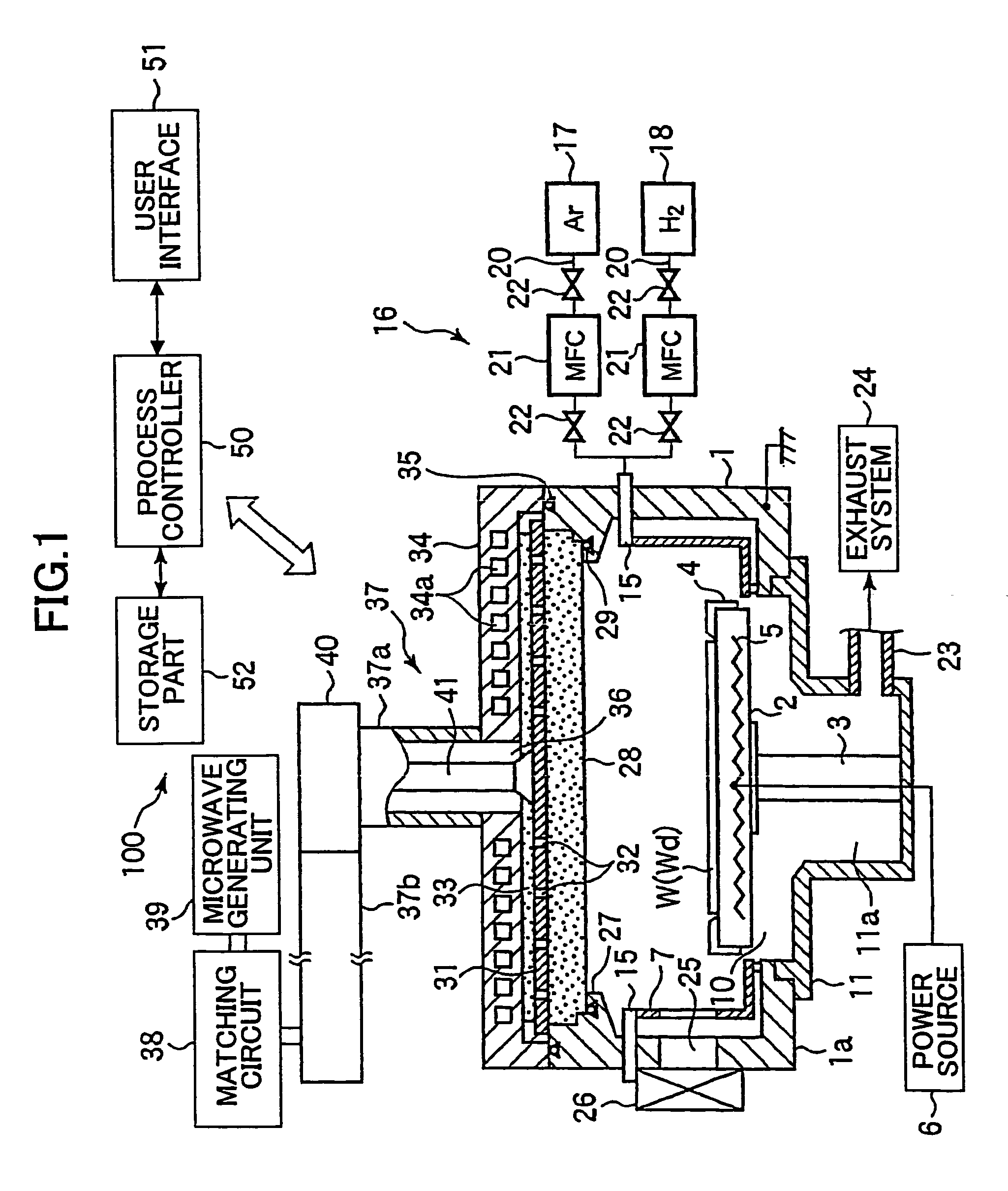
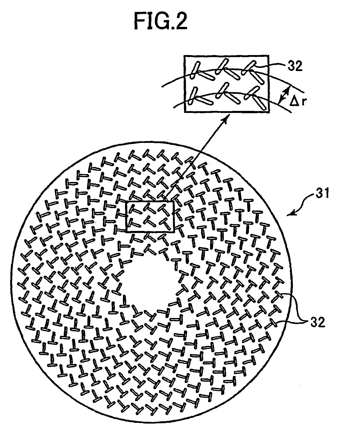
[0034]Embodiments of the present invention are described specifically with reference to figures.

[0035]As a low dielectric constant film directed to by curing processing according to the present invention, a Low-k film such as a SiOCH series film may be applied for example. In particular, according to the present invention, film curing can be achieved uniformly without an increase in a dielectric constant for a case where curing processing is carried out on a porous SiOCH series Low-k film, and thus, it is very advantageous. Further, the present invention may also be applicable for curing processing of an interlayer dielectric or such of another Low-k film, such as a SiOC series film such as a SiOC film or a porous SiOC film, a CF series film, an organic polymer series film, a MSQ series film such as a MSQ film or porous MSQ film, or such.

[0036]A thickness of the Low-k film is not limited. However, for example, one in a range of 100 to 1000 nm is preferable.

[0037]A Low-k film may be ...


PUM

PropertyMeasurementUnit
pressureaaaaaaaaaa
flow rateaaaaaaaaaa
temperatureaaaaaaaaaa

Abstract

A plasma processing method of carrying out curing processing on a low dielectric constant film produced on a to-be-processed substrate by applying plasma thereto in a processing chamber of a plasma processing apparatus, includes the steps of: a) introducing, in the plasma processing chamber, a first gas having a function of stabilizing plasma and a second gas generating active hydrogen, and, after that; b) generating plasma, and carrying out curing processing on the low dielectric constant film.

Description

BACKGROUND OF THE INVENTION[0001]1. Field of the Invention[0002]The present invention relates to a plasma processing method for processing a to-be-processed substrate such as a semiconductor substrate with the use of plasma, and a film forming method.[0003]2. Description of the Related Art[0004]In recent high-speed logic devices, reduction in dielectric constant (or obtaining Low-k) has been proceeded with, for the purpose of reducing interconnection capacitance. Further, study has been made for application of a porous material having large porosity for a very large-scale integrated circuit, and in particular, for a low dielectric constant film (i.e., a Low-k film) applied after a 65 nm technology node. Generally speaking, mechanical strength of such a porous Low-k film is low, and therefore, film peeling may occur, when copper is embedded and flattening is carried out in CMP after the Low-k film is produced. In order to avoid it, curing processing is previously required for the Low...

Claims


Application Information

Patent Timeline
Patent Type & Authority Patents(United States)
IPC IPC(8): H05H1/00C23C16/00
CPCC23C16/401C23C16/56H01J37/3222H01J37/32935H01L21/02126H01L21/02274H01L21/0234H01L21/31058H01L21/31633H01L21/76826H01L21/3122H01L21/3124
Inventor KOHNO, MASAYUKISASAKI, MASARU
Owner TOKYO ELECTRON LTD
Why Eureka
Try Eureka