Program-controlled dicing of a substrate using a pulsed laser

a pulsed laser and dicing technology, applied in the direction of manufacturing tools, metal working equipment, welding/soldering/cutting articles, etc., can solve the problems of low yield, inability to machine thin wafers, and use of mechanical saws, so as to facilitate the dicing of substrates and maximize the machining rate

Inactive Publication Date: 2010-08-17
XSIL TECH
View PDF12 Cites 147 Cited by
  • Summary
  • Abstract
  • Description
  • Claims
  • Application Information

AI Technical Summary

Benefits of technology

[0004]According to a fist aspect of the invention, there is provided a method of using a pulsed laser for program-controlled dicing of a substrate comprising at least one layer, the method comprising the steps of: providing program control means and associated data storage means for controlling the pulsed laser, providing in the associated data storage means a laser cutting strategy file of at least one selected combination of pulse rate, pulse energy and pulse spatial overlap of pulses produced by the laser at the substrate to restrict damage to the respective at least one layer while maximising machining rate for the at least one layer, providing in the laser cutting strategy file data representative of at least one selected plurality of scans of the respective at least one layer by the pulsed laser necessary to cut through the respective at least one layer when the pulsed laser is operating according to the respective at least one combination stored in the laser cutting strategy file; and using the laser under control of the program control means driven by the laser cutting strategy file to scan the at least one layer with the respective at least one selected plurality of scans at least to facilitate dicing of the substrate such that a resultant die has at least a predetermined die strength and a yield of operational die equals at least a predetermined minimum yield.
[0005]Preferably, the steps of providing a laser cutting strategy file comprise, for each of the at least one layer, the steps of varying at least one of a combination of pulse rate, pulse energy, pulse spatial overlap to provide a respective combination; measuring a cutting rate of the respective layer using the respective combination; examining the layer to determine whether damage is restricted to a predetermined extent; dicing the substrate and measuring yield of the resultant die; measuring die strength of the resultant die; creating a laser cutting strategy file of a selected combination which maximises cutting rate while resulting in a yield of operational die which have at least the predetermined minimum yield and for which the die have at least the predetermined die strength scanning the at least one layer using the selected combination to determine a plurality of scans necessary to cut though the layer; and storing the selected plurality of scans in the laser cutting strategy file.

Problems solved by technology

Use of a mechanical saw has disadvantages such as low yield, chipping and cracking.
Thin wafers cannot be machined due to the stresses induced in the wafer by the saw resulting in low die strength.
The strength of the dies produced when a semiconductor substrate is diced is an important factor as low die strengths reduce reliability.

Method used


Image

  • Program-controlled dicing of a substrate using a pulsed laser
  • Program-controlled dicing of a substrate using a pulsed laser
  • Program-controlled dicing of a substrate using a pulsed laser

Examples


Embodiment Construction

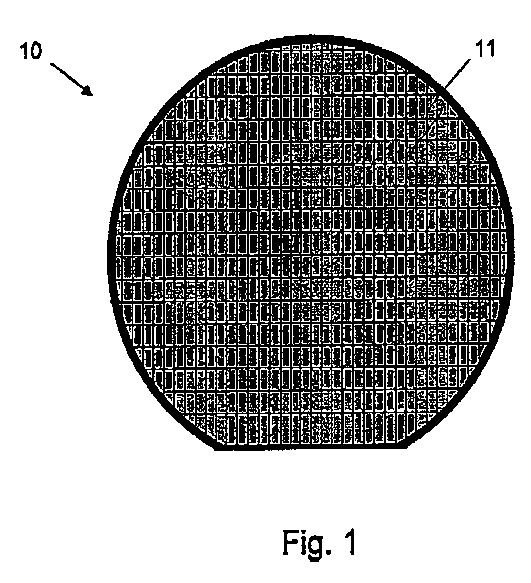
[0070]A laser beam may be used to dice a semiconductor wafer 10 and thereby singulate devices 11 from the wafer by scanning a Q-switched laser beam over the wafer surface using rotating mirrors in a galvanometer type system to form a pattern such as that shown in FIG. 1. Focusing of the laser beam may be achieved using a telecentric type scan lens.

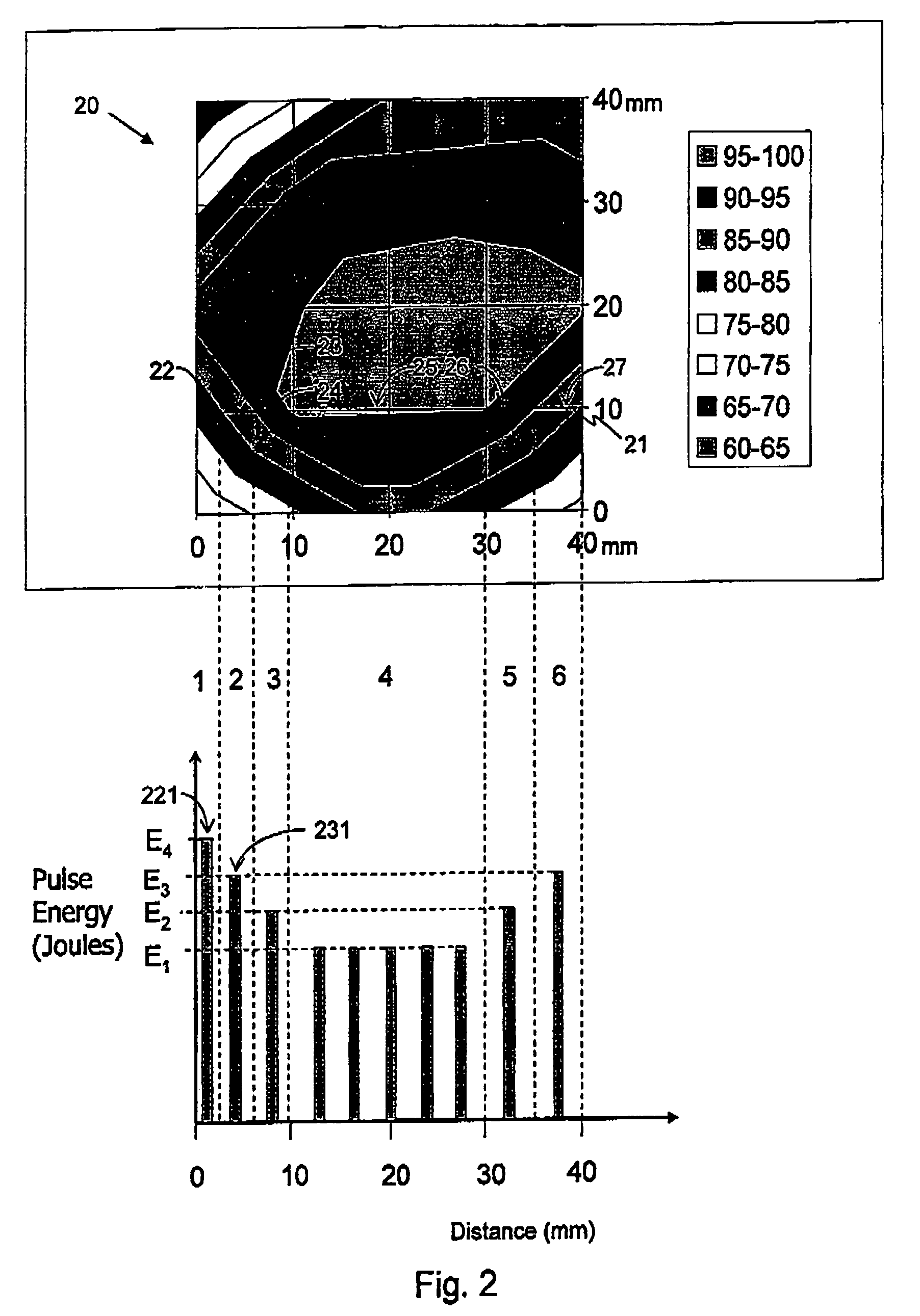
[0071]In embodiments of this invention, the temporal separation of consecutive laser pulses (Δt) and the laser pulse energy (E) is varied during machining of a single or multilayered substrate in order to reduce thermal loading in different portions of the single layer or in each of the materials in the substrate and the subsequent mechanical stress or damage that results.

[0072]By way of example, a multilayered material workpiece 30 consisting of four layers 31, 32, 33 and 34 of three different material types is shown in FIG. 3(i). These materials could be, for example, a polymer material first layer 31 on a metal second layer 32 on a poly...


PUM

PropertyMeasurementUnit
depthaaaaaaaaaa
lengthaaaaaaaaaa
lengthaaaaaaaaaa

Abstract

A substrate is diced using a program-controlled pulsed laser beam apparatus having an associated memory for storing a laser cutting strategy file. The file contains selected combinations of pulse rate Deltat, pulse energy density E and pulse spatial overlap to machine a single layer or different types of material in different layers of the substrate while restricting damage to the layers and maximising machining rate to produce die having predetermined die strength and yield. The file also contains data relating to the number of scans necessary using a selected combination to cut through a corresponding layer. The substrate is diced using the selected combinations. Gas handling equipment for inert or active gas may be provided for preventing or inducing chemical reactions at the substrate prior to, during or after dicing.

Description

[0001]This application is a U.S. National Phase of International Patent Application Serial No. PCT / EP03 / 04069, filed Apr. 17, 2003 which claims priority to Irish Patent Application No. S2002 / 0289 filed Apr. 19, 2002 and Great Britain Application No. 0225033.0 filed Oct. 28, 2002.TECHNICAL FIELD[0002]The invention relates to program-controlled dicing of a substrate, particularly, but not limited to, a semiconductor substrate, using a pulsed laser.BACKGROUND ART[0003]Wafer dicing is a critical aspect of package assembly that facilitates all subsequent operations in an assembly process. Wafer dicing is conventionally achieved by dicing a wafer with a mechanical saw. Use of a mechanical saw has disadvantages such as low yield, chipping and cracking. Thin wafers cannot be machined due to the stresses induced in the wafer by the saw resulting in low die strength. The strength of the dies produced when a semiconductor substrate is diced is an important factor as low die strengths reduce re...

Claims


Application Information

Patent Timeline
Patent Type & Authority Patents(United States)
IPC IPC(8): H01L21/00B23K26/06B23K26/38B23K101/40H01L21/301H01L21/78H05K3/00
CPCB23K26/0648B23K26/123B23K26/126H01L21/78B23K26/4075B23K2201/40B23K26/40B23K2101/40B23K2103/50
Inventor BOYLE, ADRIANMEIGHAN, OONAGH
Owner XSIL TECH
Why Eureka
Try Eureka