Isolating and moving single atoms using silicon nanocrystals

a technology of silicon nanocrystals and single atoms, applied in the field of nanocrystals, can solve problems such as extremely difficult currents

Active Publication Date: 2010-09-07
NAT TECH & ENG SOLUTIONS OF SANDIA LLC
View PDF5 Cites 5 Cited by
  • Summary
  • Abstract
  • Description
  • Claims
  • Application Information

AI Technical Summary

Benefits of technology

[0008]The method can further comprise a step of separating with an atomic force microscope tip at least one of the silicon nanocrystals containing the single atom of the atomic species of interest from the silicon nanocrystals containing the different number of atoms of the atomic species of interest. In...

Problems solved by technology

This is currently extremely difficult due to the small size of...

Method used


Image

  • Isolating and moving single atoms using silicon nanocrystals
  • Isolating and moving single atoms using silicon nanocrystals
  • Isolating and moving single atoms using silicon nanocrystals

Examples


Embodiment Construction

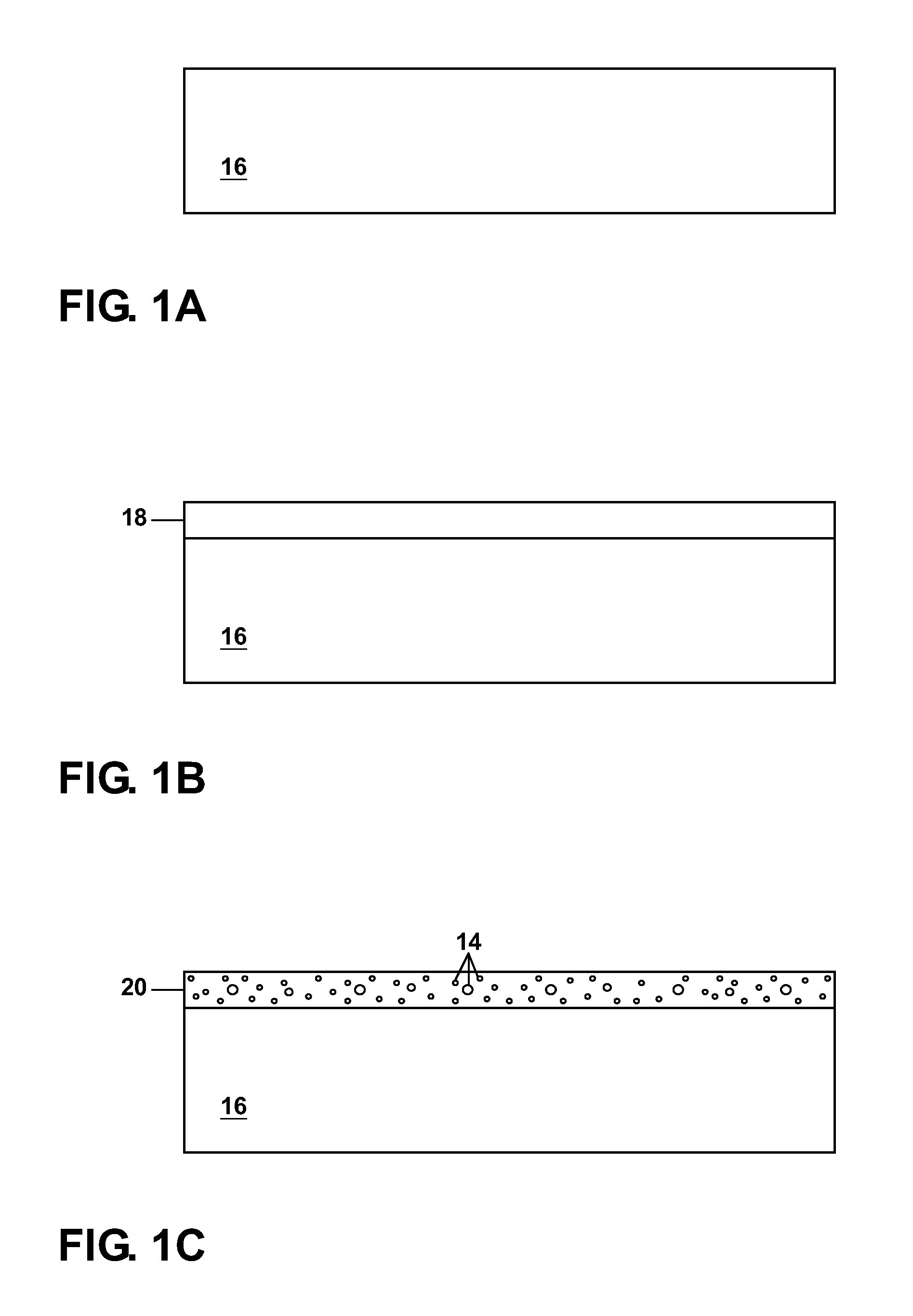
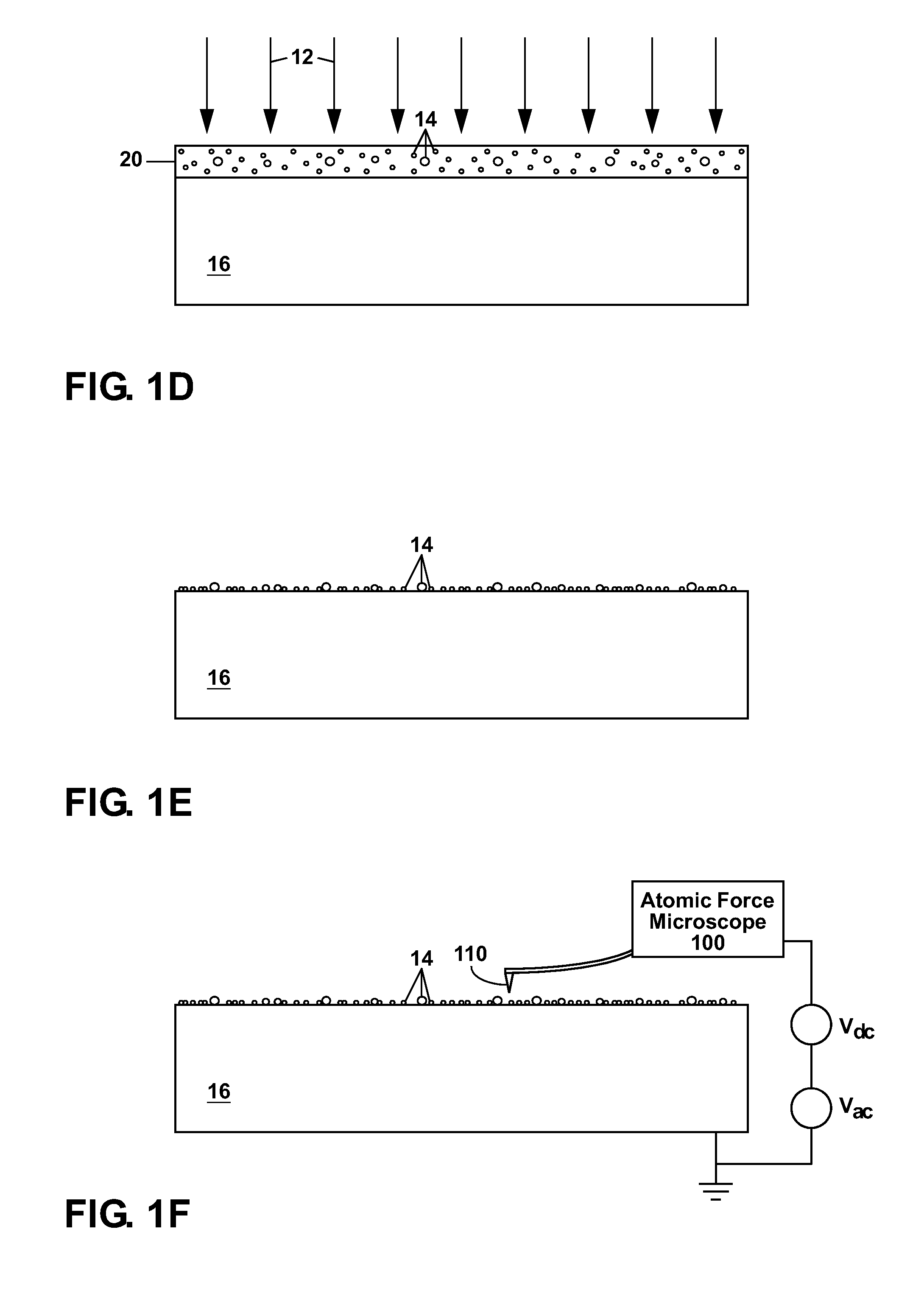
[0021]Isolating single atoms 12 of an atomic species of interest according to the present invention requires silicon nanocrystals 14 into which the single atoms can be placed. The silicon nanocrystals 14 can either be procured commercially or can be fabricated as described in detail hereinafter with reference to FIGS. 1A-1G which schematically illustrate in cross-section views a series of steps for forming the silicon nanocrystals 14 on a substrate 16. The term “nanocrystal” as used herein refers to an assembly of atoms with an at least partially crystalline structure and having overall dimensions of about 100 nanometers or less.

[0022]In FIG. 1A, the substrate 16 can comprise a conventional semiconductor substrate such as a silicon substrate 16 (i.e. a silicon wafer, or a portion thereof). The silicon substrate 16 can have a {100} crystalline orientation, for example, and can be doped with boron or phosphorous to a concentration of about 1019 cm−3 or more to make the substrate 16 el...


PUM

PropertyMeasurementUnit
Temperatureaaaaaaaaaa
Nanoscale particle sizeaaaaaaaaaa
Electrical conductoraaaaaaaaaa

Abstract

A method is disclosed for isolating single atoms of an atomic species of interest by locating the atoms within silicon nanocrystals. This can be done by implanting, on the average, a single atom of the atomic species of interest into each nanocrystal, and then measuring an electrical charge distribution on the nanocrystals with scanning capacitance microscopy (SCM) or electrostatic force microscopy (EFM) to identify and select those nanocrystals having exactly one atom of the atomic species of interest therein. The nanocrystals with the single atom of the atomic species of interest therein can be sorted and moved using an atomic force microscope (AFM) tip. The method is useful for forming nanoscale electronic and optical devices including quantum computers and single-photon light sources.

Description

GOVERNMENT RIGHTS[0001]This invention was made with Government support under Contract No. DE-AC04-94AL85000 awarded by the U.S. Department of Energy. The Government has certain rights in the invention.FIELD OF THE INVENTION[0002]The present invention relates in general to nanocrystals and in particular to the use of silicon nanocrystals as a way of isolating and moving single atoms of an atomic species of interest. The present invention also relates a method for inserting single atoms of an atomic species of interest into a quantum computer which is being built up on a substrate.BACKGROUND OF THE INVENTION[0003]The emerging fields of quantum computing and single-photon light sources require a precise placement of single atoms of a particular atomic species within a quantum computer or within a high-Q optical cavity, respectively. This is currently extremely difficult due to the small size of individual atoms which does not allow them to be easily manipulated. What is needed Is a way...

Claims


Application Information

Patent Timeline
IPC IPC(8): C03C15/00C03C25/68
CPCB82Y10/00B82B3/0071H01L29/127B82Y20/00H01L33/0054H01L33/06H01L33/465H01L29/7613Y10S977/858G01Q80/00Y10S977/888Y10S977/856Y10S977/855
Inventor CARROLL, MALCOLM S.
Owner NAT TECH & ENG SOLUTIONS OF SANDIA LLC
Why Eureka
Try Eureka