Semiconductor device and method of producing the same including a charge accumulation layer with differing charge trap surface density

a technology of magnetic and insulating film, which is applied in the direction of solid-state devices, transistors, instruments, etc., can solve the problems of reducing the efficiency of writing the injected electrons, and increasing the writing time. , to achieve the effect of improving the writing and erasing properties, suppressing the dispersion thereof, and improving the retention property

Inactive Publication Date: 2010-09-07
NEC CORP
View PDF11 Cites 12 Cited by
  • Summary
  • Abstract
  • Description
  • Claims
  • Application Information

AI Technical Summary

Benefits of technology

[0018]In the trap memory of the present invention, the electric charge trap immediately below the gate electrode is rendered higher in surface density than that outside the gate electrode, so that the electric charge trap immediately below the gate electrode accumulates more electric charges at the time of writing by injecting CHE to improve writing and erasing properties. The electric charges accumulated below the gate electrode are suppressed to diffuse into regions outside the gate electrode to improve the retention property. Moreover, electrons to be injected for neutralization at the time of ion implantation to form the source and the drain region are suppressed to diffuse below the gate electrode, which does not increases the initial threshold value VT and suppresses the dispersion thereof.

Problems solved by technology

Therefore, although the flash memory has mainly used a floating gate (FG) memory cell up to the 0.13 μm node era to meet requirements for reducing a cell area and thinning an insulation film, attention has been paid to a trap memory which uses traps discretely included in an insulating film to capture electric charges because it has been found that thinning the insulating film will be difficult in view of securement of retention property in the 90 nm node era or later.
The first example of the conventional trap memory has a significant problem as described below.
This reduces efficiency in writing the injected electrons to increase the writing time.
The defect remains at the gate end portion even after the gate side wall 7 has been formed to increase a leak current through the defect and cause leakage of the accumulated charge, resulting in decrease in yield.
However, a bird's beak is formed on the substrate at the gate end portion by the thermal oxidation to increase the defect density of the first gate insulating film near the gate end, lowering the yield.

Method used


Image

  • Semiconductor device and method of producing the same including a charge accumulation layer with differing charge trap surface density
  • Semiconductor device and method of producing the same including a charge accumulation layer with differing charge trap surface density
  • Semiconductor device and method of producing the same including a charge accumulation layer with differing charge trap surface density

Examples


first exemplary embodiment

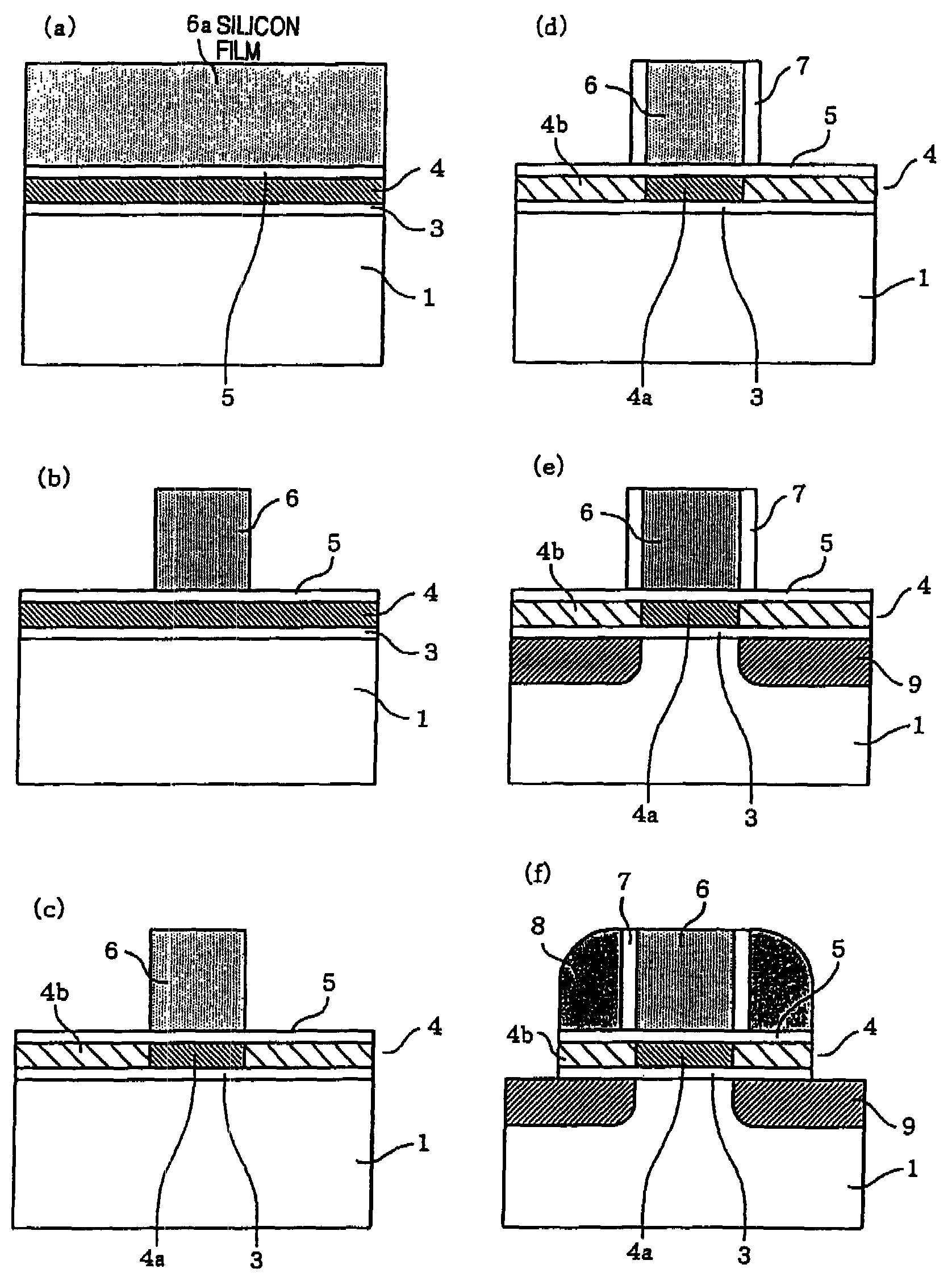
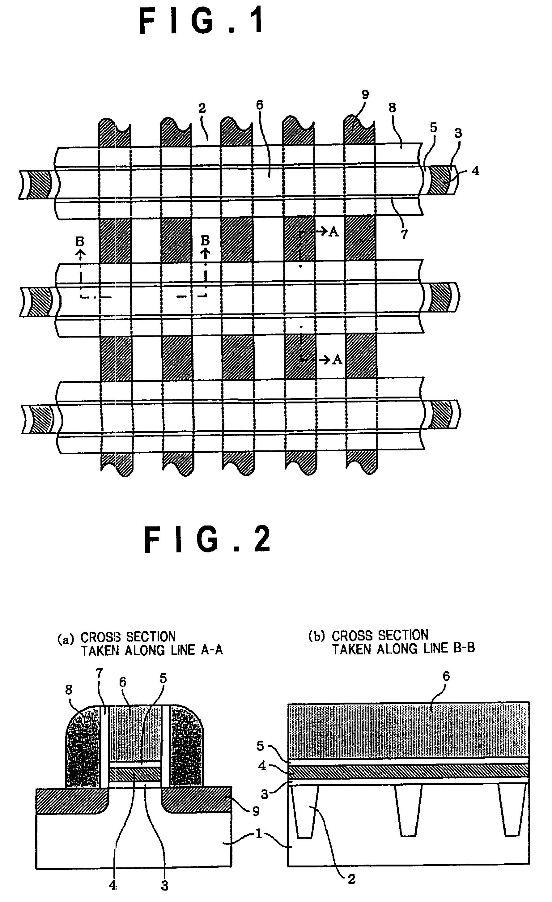
[0020]FIG. 9 is a top view of a trap memory according to the first exemplary embodiment of the present invention. FIGS. 10(a) and 10(b) are cross sections taken along lines A-A and B-B in FIG. 9. As illustrated in FIGS. 9 and 10, a plurality of element isolation insulating films 2 which segments an active region are formed in the surface region of a silicon substrate 1 so as to extend in the upper and the lower direction in FIG. 9. A laminate insulating film composed of a first gate insulating film 3, a charge accumulation layer 4 and a second gate insulating film 5 is formed over the silicon substrate 1. The predetermined number of gate conductors 6 are formed so as to be orthogonal to the active region (i.e. to be orthogonal to the element isolation insulating films 2) over the laminate insulating film. Gate side walls 7 are formed on both sides of the gate conductor 6. Side walls 8 are formed outside the gate side walls 7. An impurity diffusion layer 9 forming a source and a drai...

example 1

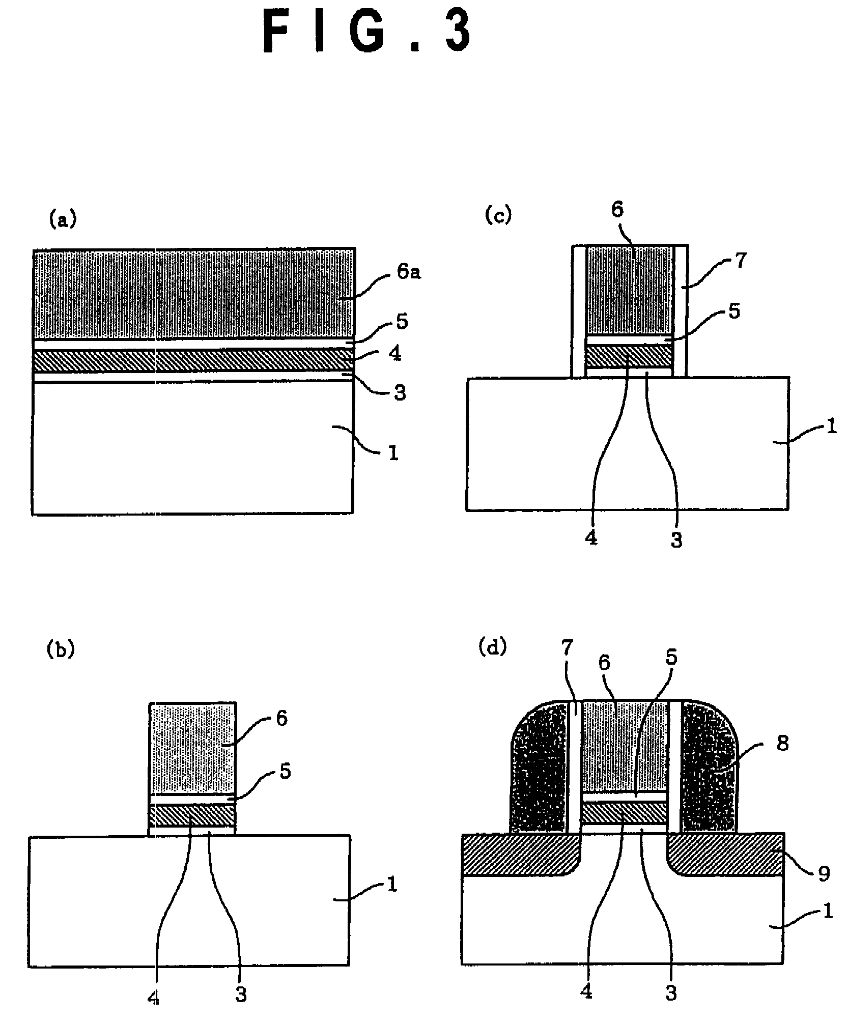
[0032]FIG. 14 is a top view of an example 1 of the present invention. FIGS. 15(a) and 15(b) are cross sections taken along lines A-A and B-B in FIG. 14. In FIGS. 14 and 15, the same portions as those in the first exemplary embodiment illustrated in FIGS. 9 and 10 are denoted by the same reference numerals as those in FIGS. 9 and 10 and the duplicated description thereof is omitted. In the present example, the portion of the charge accumulation layer 4 immediately under the gate conductor 6 is rendered the high trap surface-density region 4a, part of the outside portion of the gate conductor is rendered the low trap surface-density region 4b which is lower in trap surface-density than the high trap surface-density region 4a and the portion outside the part is rendered a non-trap region 4c which does not contain electric charge traps. The non-trap region 4c does not contain nitrogen and is almost completely converted to a silicon oxide film. In the memory cell of the example 1, electr...

example 2

[0033]FIG. 16 is a top view of an example 2 of the present invention. FIGS. 17(a) and 17(b) are cross sections taken along lines A-A and B-B in FIG. 16. In FIGS. 16 and 17, the same portions as those in the first exemplary embodiment illustrated in FIGS. 9 and 10 are denoted by the same reference numerals as those in FIGS. 9 and 10 and the duplicated description thereof is omitted. In the present example, the portion of the charge accumulation layer 4 immediately under the gate conductor 6 is rendered the high trap surface-density region 4a and the portion outside the end of the gate conductor is rendered the non-trap region 4c which does not contain electric charge traps. The non-trap region 4c outside the end of the gate conductor does not contain nitrogen and is almost completely converted to a silicon oxide film. In the memory cell of the example 2, electric charge traps do not exist at the portion outside the gate conductor. The charge accumulation layer 4 inside the gate condu...


PUM


Abstract

There is provided a trap memory device suppresses electric charges from flowing from the outside into a charge accumulation region and accumulated electric charges from diffusing to the outside or flowing out due to a defect. A gate conductor 6 is formed through a laminate insulating film including a first gate insulating film 3, a charge accumulation layer 4 and a second gate insulating film 5 on a silicon substrate 1. The laminate insulating film (3 to 5) projects outside the gate conductor 6 and extends to under the outer end of a side wall 8. The charge accumulation layer 4 includes a high trap surface-density region 4a immediately under the gate conductor and a low trap surface-density region 4b outside the gate conductor.

Description

TECHNICAL FIELD[0001]The present invention relates to a semiconductor device and a method of producing the same, and in particular, to a semiconductor device including a rewritable nonvolatile semiconductor memory typified by a flash memory and a method of producing the same.BACKGROUND ART[0002]LSIs including a flash memory continue to be miniaturized, and are entering the 65 nm era from the current 0.13 μm and 90 nm nodes era. Therefore, although the flash memory has mainly used a floating gate (FG) memory cell up to the 0.13 μm node era to meet requirements for reducing a cell area and thinning an insulation film, attention has been paid to a trap memory which uses traps discretely included in an insulating film to capture electric charges because it has been found that thinning the insulating film will be difficult in view of securement of retention property in the 90 nm node era or later. In comparison with the FG memory, the trap memory has the advantage that an effective oxide...

Claims


Application Information

Patent Timeline
Patent Type & Authority Patents(United States)
IPC IPC(8): H01L21/8238H01L31/119H01L29/76H01L21/336H01L31/113H01L31/062H01L29/94
CPCG11C16/0466H01L21/28282H01L27/115H01L27/11568H01L29/4234H01L29/66833H01L29/792H01L29/40117H10B69/00H10B43/30
Inventor TERAI, MASAYUKI
Owner NEC CORP
Why Eureka
Try Eureka