Liquid crystal display on a printed circuit board
a printed circuit board and liquid crystal display technology, applied in static indicating devices, instruments, non-linear optics, etc., can solve the problems of complicated, fragile and problematic components, difficult interconnection, and labor-intensive interconnections between drive electronics and display cells, and achieve simplified lcd manufacturing processes and lower costs.
- Summary
- Abstract
- Description
- Claims
- Application Information
AI Technical Summary
Benefits of technology
Problems solved by technology
Method used
Image
Examples
example 1
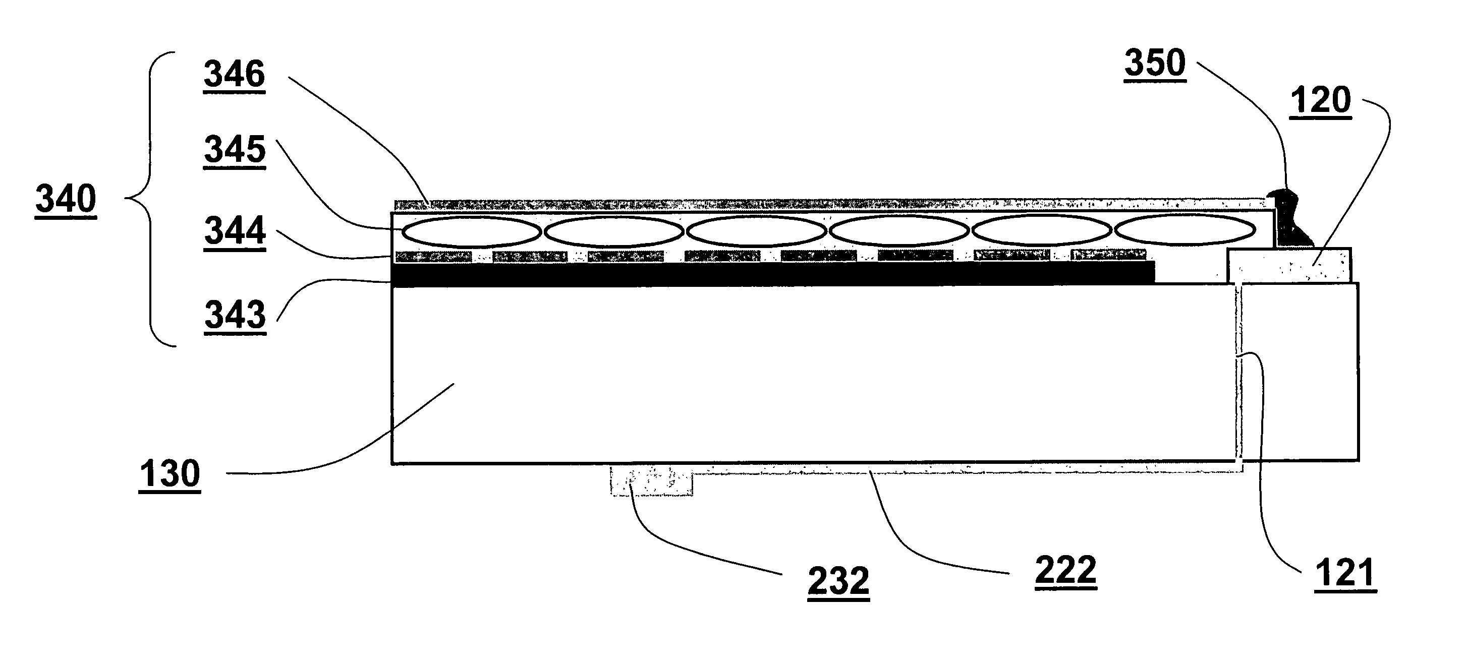
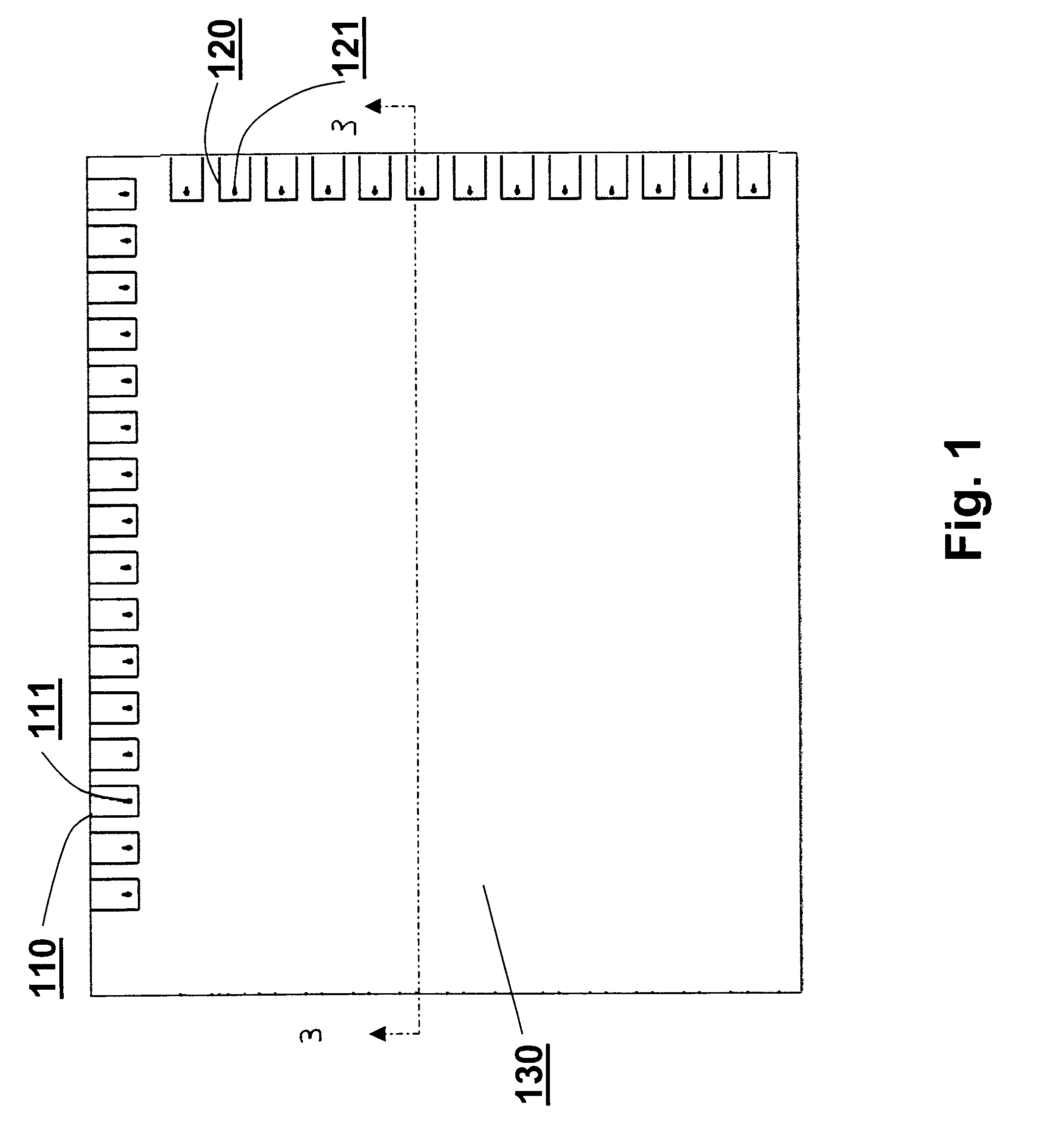
[0038]An operable 13×16 pixel passive matrix cholesteric display was made by coating and printing the various display elements on a plastic substrate with back pressure sensitive adhesive (PSA) layer and release liner. The plastic substrate was a PET sheet with a thickness of 12.5 microns available from Grafix (Cleveland). A layer of conducting polymer (ELP-3040 available from Agfa-Gevaert, Belgium) was screen printed on the plastic substrate as 5 mm wide, 15 cm long electrode strips spaced 1 mm apart to serve as the column electrodes of the passive matrix display. After casting, the conducting polymer was cured at 100° C. for 10 minutes. A layer of encapsulated cholesteric liquid crystal in polymer binder was coated from a water-based emulsion on the conducting polymer layer using a doctor blade having a 25 micron (μm) gap and allowed to dry for 1 hour at room temperature. The thickness of the encapsulated liquid crystal layer was approximately 8-10 μm. The emulsion was prepared fr...
example 2
[0040]The following is an example of preparation of the coated cholesteric display directly on the PCB. The display had the same sequence of layers as in Example 1 except that the 12.5 μm PET with PSA and release liner were replaced by the PCB. All display layers including bottom conducting polymer electrodes, encapsulated liquid crystal, top conducting polymer electrodes and clear coat were sequentially coated directly on the PCB as a substrate.
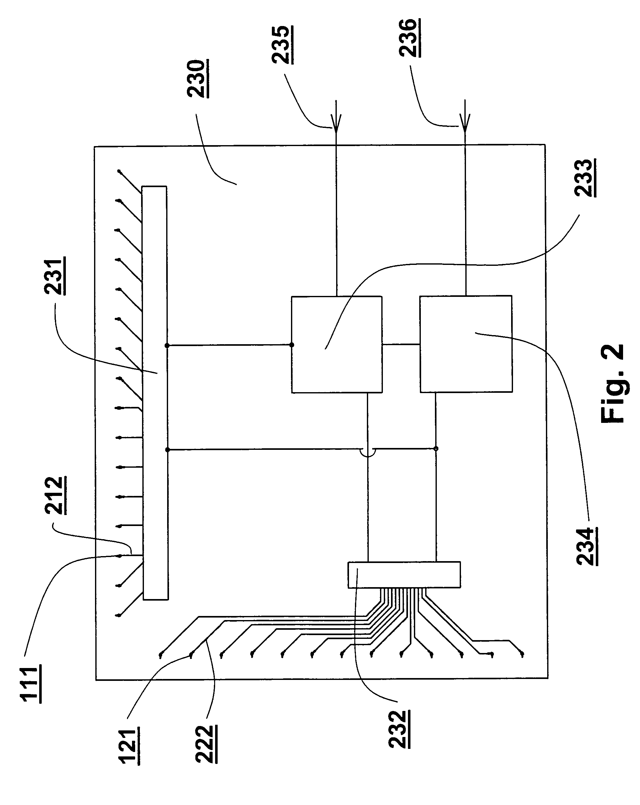
[0041]The top conducting polymer electrodes were connected to the PCB pads as in Example 1. The bottom conducting polymer electrodes were connected to the driving electronics through vias in the PCB.
PUM
| Property | Measurement | Unit |
|---|---|---|
| thickness | aaaaa | aaaaa |
| thickness | aaaaa | aaaaa |
| thickness | aaaaa | aaaaa |
Abstract
Description
Claims
Application Information


