Polar modulation transmitter circuit and communications device

a transmitter circuit and polar modulation technology, applied in the field of transmitter circuits, can solve the problems of increasing device size and power dissipation, low power efficiency of linear amplifiers, and short operating time, and achieve the effects of low distortion, high efficiency, and suppressing distortion

Inactive Publication Date: 2010-09-07
PANASONIC CORP
View PDF7 Cites 17 Cited by
  • Summary
  • Abstract
  • Description
  • Claims
  • Application Information

AI Technical Summary

Benefits of technology

[0016]The regulator may be a switching regulator. This allows the transmitter circuit to operate with high efficiency.
[0018]Preferably, the signal generation section further outputs power information which is set based on a base band section of the transmitter circuit. In this case, the regulator includes a switching regulator and a series regulator. The switching regulator supplies to the series regulator a voltage controlled by the power information. The series regulator outputs, while applying the voltage supplied from the switching regulator, a signal in accordance with a magnitude of the signal which has been wave-shaping-processed by the compensating filter. This allows a reduction in a loss at the series regulator and in power consumption.
[0019]Preferably, a transfer characteristic of the compensating filter is constant irrespective of a magnitude of the amplitude signal. When the signal generation section further outputs the power information which is set based on the base band section of the transmitted circuit, the transfer characteristic of the compensating filter may be changed in accordance with a magnitude of the power information. This allows the transmitter circuit to suppress distortion caused by insufficient frequency bandwidth of the regulator and the amplitude modulator section irrespective of a magnitude of the transmitted signal outputted by the amplitude modulator section.
[0021]As described above, according to the present invention, the compensating filter compensates the amplitude signal outputted by the signal generation section so as to have an inverse characteristic of a transfer characteristic between an input at the regulator and an output at the amplitude modulator section, thereby suppressing distortion caused by insufficient frequency bandwidth of the regulator and the amplitude modulator section. Thus, the transmitter circuit is capable of outputting a transmitted signal with low distortion and high efficiency even in a modulation method in which modulation bandwidth is wide.
[0022]And the transmitter circuit further includes a predistortion section for compensating non-linearity of at least any of the angle modulator section, the regulator, and the amplitude modulator section. The predistortion section compensates non-linearity of at least any of the angle modulator section, the regulator, and the amplitude modulator section, and thereby suppresses the distortion caused by the insufficient frequency bandwidth of the regulator and the amplitude modulator section, thus making it possible to output a transmitted signal having the distortion reduced.
[0023]In addition, according to a communications device of the present invention, the communications device, by using the transmitter circuit described above, is capable of ensuring an accuracy of an outputted signal in wide bandwidth and operating while achieving high efficiency and downsizing.

Problems solved by technology

Whereas these linear amplifiers are excellent in linearity, power efficiency of the linear amplifiers is low as compared with Class C to E non-linear amplifiers.
Consequently, when these radio frequency power amplifiers are applied to a mobile communications device whose power source is a battery, due to a large power consumption of the radio frequency power amplifiers, there accrues a problem of a shorter operating time.
In addition, when these radio frequency amplifiers are applied to a base station device of a wireless system in which a plurality of transmitter circuits outputting a large amount of power are mounted, problems of increases in size of the device and in power dissipation will arise.
In recent years, however, wider modulation bandwidth of a transmitter circuit has been desired and consequently, it is anticipated that frequency bandwidth of the regulator 504 and the amplitude modulator section 505 would become insufficient.
Judging from this result, it turns out that even when a delay time, caused by a difference in paths, between the amplitude signal and the phase signal is adjusted, ACPs cannot be sufficiently reduced and an optimum delay time for ACPs depends on detuning, making it difficult to sufficiently reduce all ACPs.

Method used


Image

  • Polar modulation transmitter circuit and communications device
  • Polar modulation transmitter circuit and communications device
  • Polar modulation transmitter circuit and communications device

Examples


first embodiment

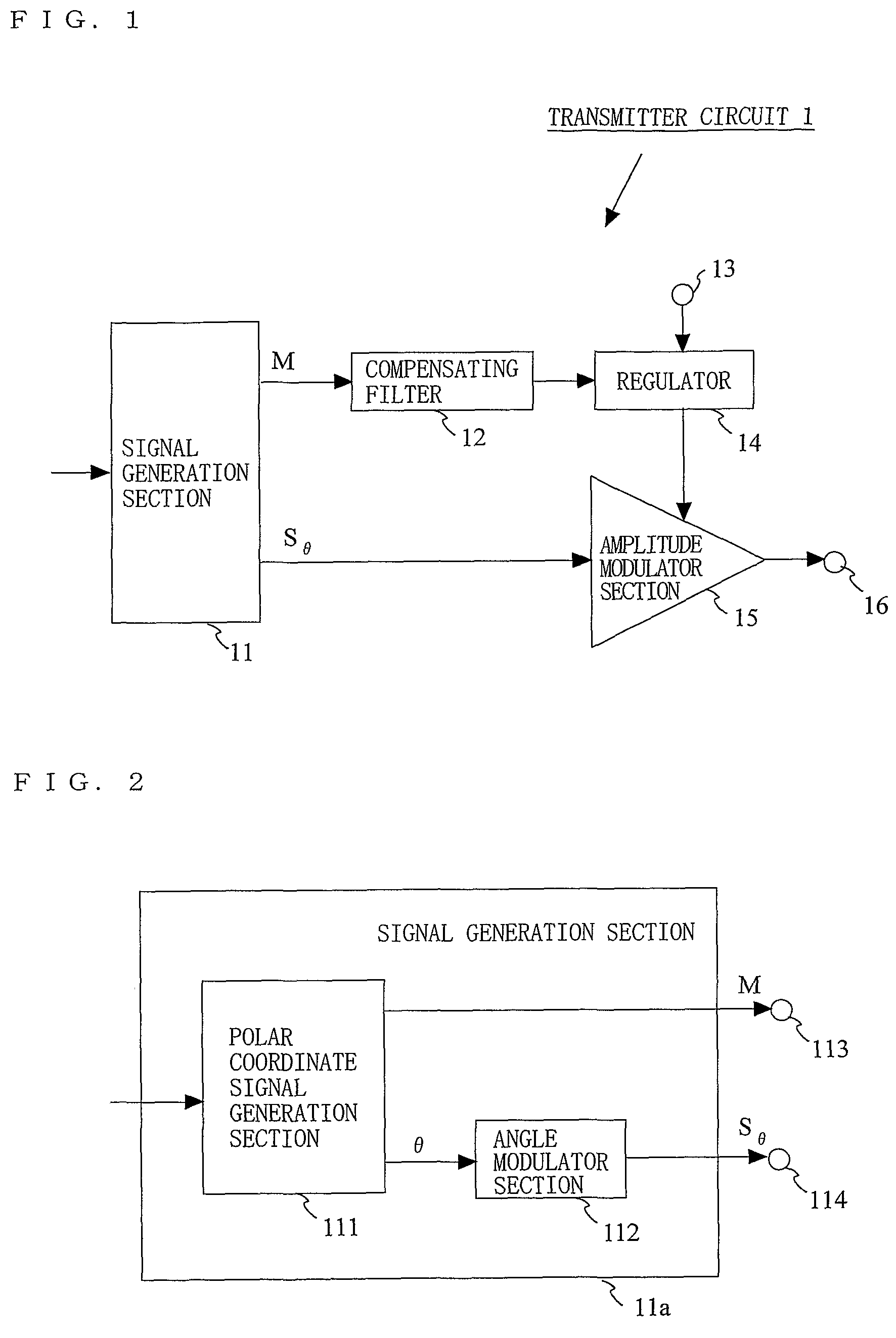
[0056]FIG. 1 is a block diagram illustrating an exemplary configuration of a transmitter circuit 1 according to a first embodiment of the present invention. In FIG. 1, the transmitter circuit 1 includes a signal generation section 11, a compensating filter 12, a power source terminal 13, a regulator 14, an amplitude modulator section 15, and an output terminal 16. The signal generation section 11, based on an amplitude component and a phase component obtained by signal-processing input data, outputs an amplitude signal M and an angle-modulated signal Sθ. The amplitude signal M is wave-shaping-processed and thereafter is inputted to the regulator 14. The regulator 14 outputs a signal controlled by the inputted amplitude signal. Typically, the regulator 14 outputs a signal in proportion to a magnitude of the inputted amplitude signal. The signal outputted by the regulator 14 is inputted to the amplitude modulator section 15.

[0057]The angle-modulated signal Sθ is inputted to the amplit...

second embodiment

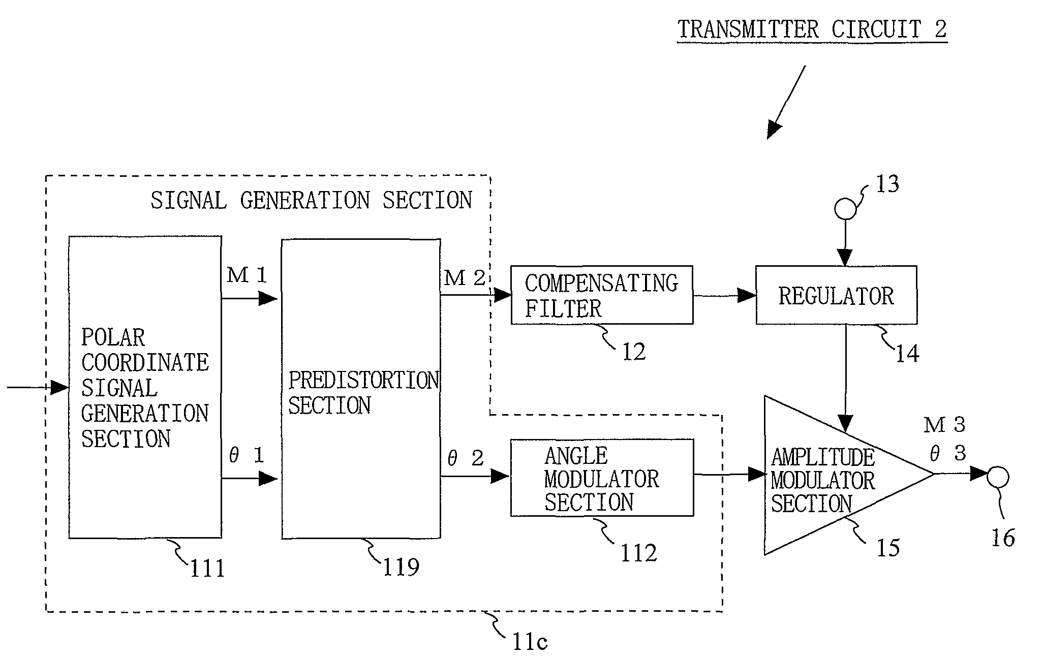
[0087]FIG. 14A is a block diagram illustrating an exemplary configuration of a transmitter circuit 2 according to a second embodiment of the present invention. In FIG. 14A, the transmitter circuit 2 includes a signal generation section whose configuration is different from that in the first embodiment. The signal generation section 11c includes a polar coordinate signal generation section 111, a predistortion section 119, and an angle modulator section 112. In FIG. 14A, the predistortion section 119 compensates an amplitude signal M1 and a phase signal θ1 which are generated by the polar coordinate signal generation section 111 so as to suppress distortion caused in at least any of a regulator 14, an angle modulator section 112, and an amplitude modulator section 15.

[0088]Specifically, the predistortion section 119 distorts a previously inputted signal using a predistortion table so as to have an inverse characteristic of a magnitude (AM / AM characteristic) of an envelope of a transm...

third embodiment

[0094]FIG. 18 is a block diagram illustrating an exemplary configuration of a transmitter circuit 3 according to a third embodiment of the present invention. In FIG. 18, in the transmitter circuit, a signal generation section 11c and a regulator 14d are different from those in the transmitter circuit 1 according to the first embodiment of the present invention. Unlike in the transmitter circuit 1 according to the first embodiment, the signal generation section 11c further outputs power information P which is set based on a base band section of the transmitter circuit 3. The regulator 14d includes a series regulator 14a and a switching regulator 14b. A configuration of the series regulator 14a, for example, is shown in FIG. 14. A configuration of the switching regulator 14b, for example, is shown in FIG. 5.

[0095]The power information, for example, in a case of a W-CDMA system, is controlled by a base station. In other words, required power is sent from the base station to the transmi...


PUM


Abstract

Provided is a transmitter circuit capable of operating with low distortion and high efficiency even in a modulation method using wide modulation bandwidth. In the transmitter circuit, a signal generation section (11) generates an amplitude signal and an angle-modulated signal. Based on a predetermined characteristic, a compensating filter (12) wave-shaping-processes the amplitude signal. A regulator (14) outputs a signal in accordance with a magnitude of the signal which has been wave-shaping-processed by the compensating filter (12). An amplitude modulator section (15) amplitude-modulates the angle-modulated signal by using the signal outputted from the regulator (14). A characteristic of the compensating filter (12) is an inverse of a transfer characteristic between an input at the regulator (14) and an output at the amplitude modulator section (15).

Description

TECHNICAL FIELD[0001]The present invention relates to a transmitter circuit for use in a communications device such as a mobile telephone, a wireless LAN device, and the like and more particularly, to a transmitter circuit capable of outputting a transmitted signal with low distortion and high efficiency in a modulation method which has wide modulation bandwidth and a communications device using the transmitter circuit.BACKGROUND ART[0002]Conventionally, as a radio frequency power amplifier for amplifying a modulated signal with varying envelope, Class A or Class AB linear amplifier had been used in order to amplify the signal with varying envelope in a linear manner. Whereas these linear amplifiers are excellent in linearity, power efficiency of the linear amplifiers is low as compared with Class C to E non-linear amplifiers. Consequently, when these radio frequency power amplifiers are applied to a mobile communications device whose power source is a battery, due to a large power ...

Claims


Application Information

Patent Timeline
Patent Type & Authority Patents(United States)
IPC IPC(8): H04K1/02H04L25/03H04L25/49
CPCH03F1/02H03F1/0205H03F1/3241H03F3/191H03F3/24H03G3/004H04L27/361H04L27/368H03F2200/331
Inventor MATSUURA, TORUMORIMOTO, SHIGERU
Owner PANASONIC CORP
Why Eureka
Try Eureka