Semiconductor device

a technology of semiconductor devices and semiconductors, applied in the field of semiconductor devices, can solve the problems of increasing the burden on the column selection line ys, signal delay becomes a problem, and the burden on the column selection line b>7/b>, and achieves the effect of increasing the precharge speed of data i/o lines and increasing the speed of reading data

Active Publication Date: 2010-09-14
LONGITUDE LICENSING LTD
View PDF4 Cites 382 Cited by
  • Summary
  • Abstract
  • Description
  • Claims
  • Application Information

AI Technical Summary

Benefits of technology

[0030]The present invention was achieved in view of the above circumstances, and has as its object to provide a semiconductor device that increases the precharge speed of data I / O lines or data amplifier without increasing the consumption current, and increases the speed of reading data from memory and the speed of writing data to memory.

Problems solved by technology

For that reason, the burden on the column selecting line 7 increases, and signal delay becomes a problem.
For this reason, the burden on the column selecting line YS further increases, and the signal delay becomes greater.
However, in the state of outputting data to the output buffer 75, it is not possible to perform precharging of the data I / O line that has already completed the process of transmitting data to the data amplifier.
For this reason, due to a reduction in the differential voltage of the data I / O line pair during driving of the data amplifier, a speed reduction in the amplification operation of the data amplifier results, serving as a cause of rate limit of the data read clock cycle.
Moreover, due to the differential voltage of the I / O data line pair prior to precharge, the previous differential voltage is not completely dissolved, and so may lead to a malfunction of outputting data that differs from the actual data.
Similarly to in the read mode, at the point in which the write amplifier has been enabled, precharging has not been completely completed, which may cause a reduction in the writing sneed.

Method used


Image

  • Semiconductor device
  • Semiconductor device
  • Semiconductor device

Examples


Embodiment Construction

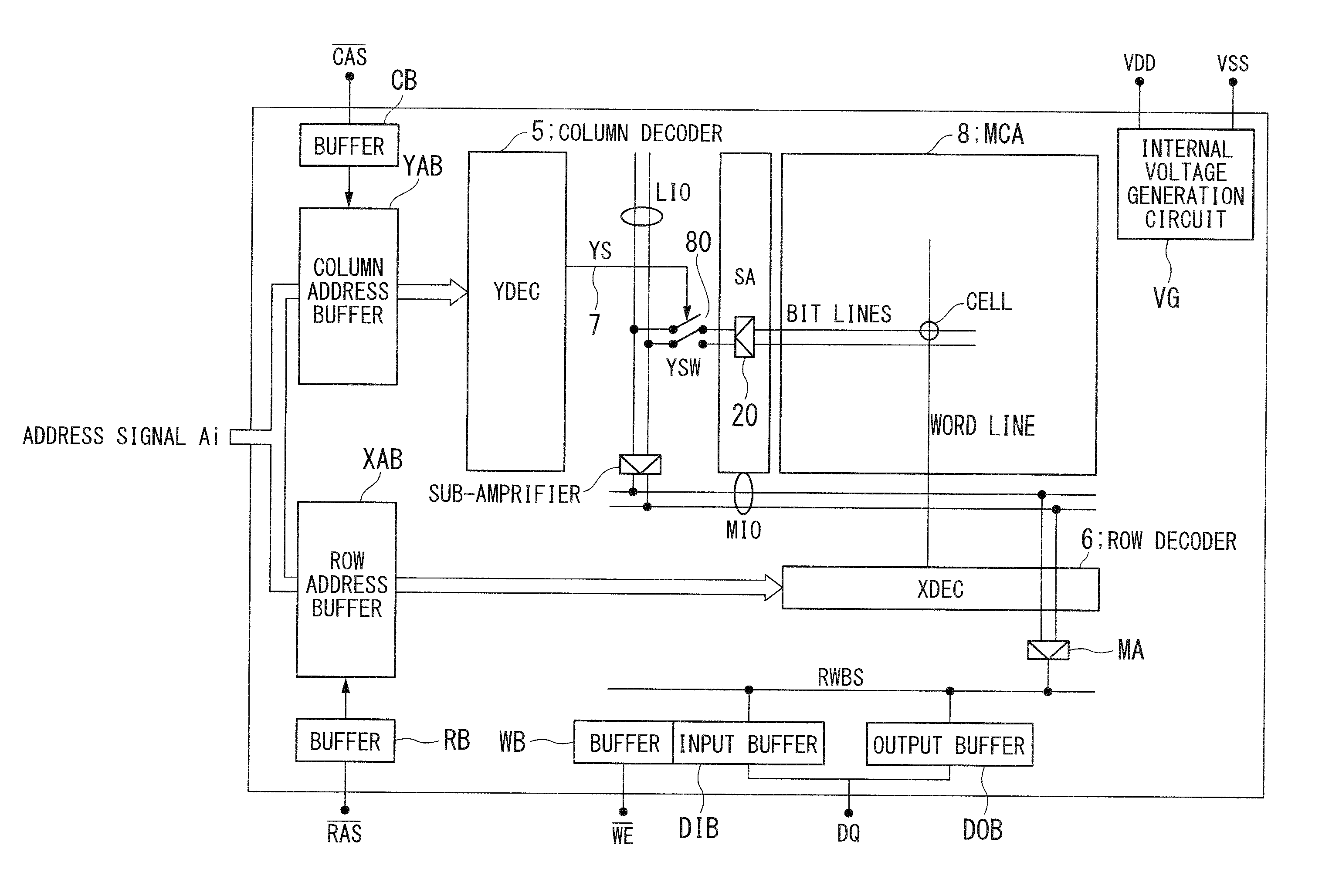
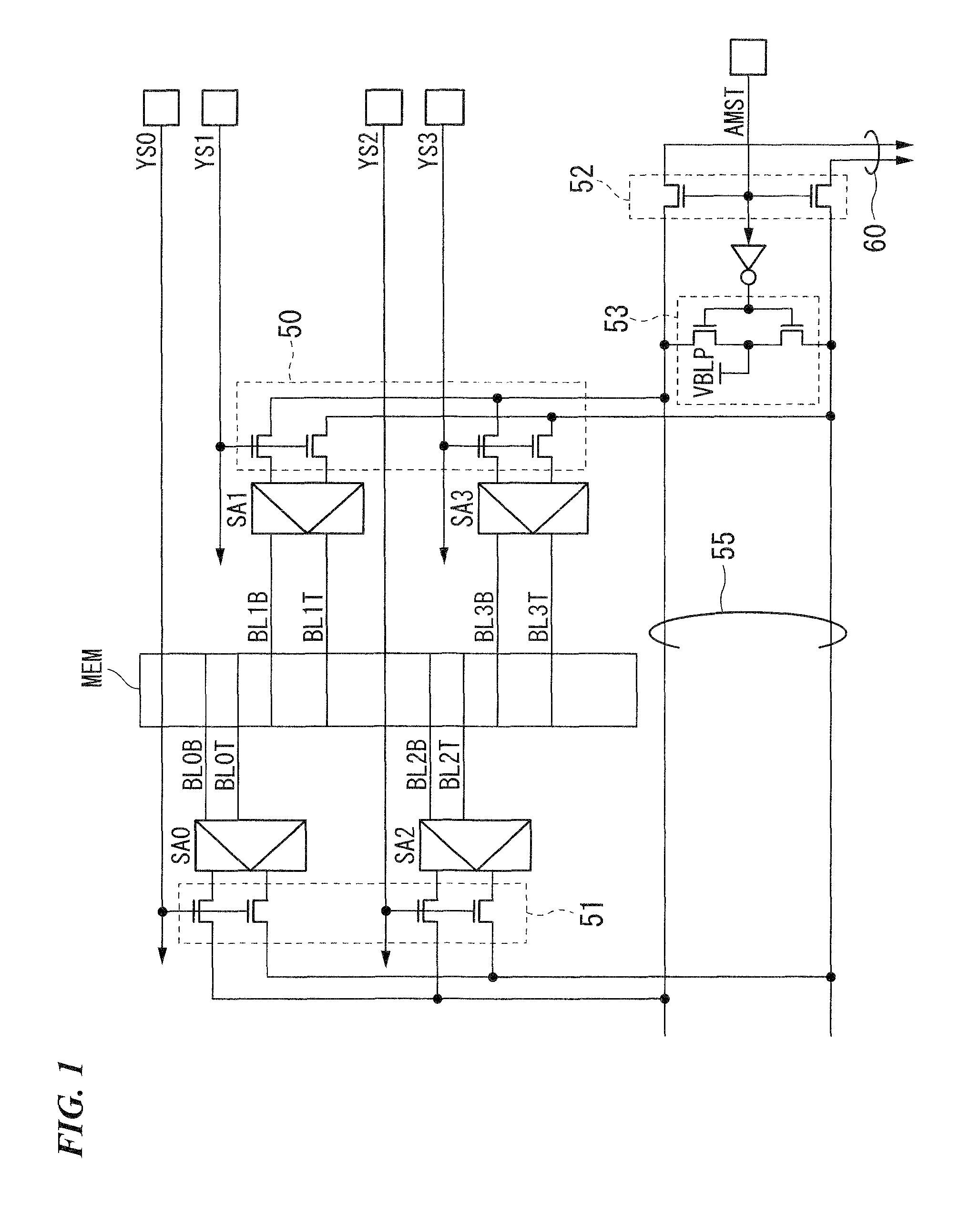
[0053]An embodiment of the present invention will be described hereinbelow with reference to the drawings. The overall constitution of the semiconductor device is the same as that illustrated in FIG. 9 that has already described. FIG. 1 is a block diagram that shows a configuration example of a memory cell array in an embodiment of the present invention.

[0054]In the drawing, a memory region MEM is connected to each bit line pair. A bit line pair BL1T and BL1B is connected to a sense amplifier SA1. A bit line pair BL3T and BL3B is connected to a sense amplifier SA3. A bit line pair BL0T and BL0B is connected to a sense amplifier SA0. A bit line pair BL2T and BL2B is connected to a sense amplifier SA2.

[0055]Any of the aforementioned plurality of bit line pairs connects to a local I / O line pair 55 by bit line selecting switches 50 and 51 (for example, a Y switch that is a column selecting switch that is constituted by an n-channel type MOS transistor). A precharge circuit 53 that perfo...


PUM


Abstract

A semiconductor device includes a column decoder that generates a column selecting signal that selects any of a plurality of bit line pairs to which memory cells are connected according to a column address that is input; a bit line selecting switch that connects by the column selecting signal any of a plurality of bit line pairs and a data I / O line pair that outputs data that has been read from a memory cell to the outside; a data amplifier that amplifies a voltage differential of a data I / O line pair and outputs data that has been read to an output buffer; a data I / O line switch that is provided in the data I / O lines; an I / O line precharge circuit that precharges a data I / O line pair that is not on the side of the data amplifier; and an amplifier precharge circuit that precharges a data I / O line pair that is on the side of the data amplifier.

Description

BACKGROUND OF THE INVENTION[0001]1. Field of the Invention[0002]The present invention relates to a semiconductor device that performs high-speed access by dividing a memory cell array into a plurality of banks in which memory cells mutually operate independently.[0003]Priority is claimed on Japanese Patent Application No. 2007-171979, filed Jun. 29, 2007, the content of which is incorporated herein by reference.[0004]2. Description of Related Art[0005]In recent years, a dynamic random access memory (DRAM) has seen advances in terms of higher capacities, higher speeds, and lower power consumption. In particular, there has been intense demand for higher data transfer speeds, leading to the proposal of new architectures such as double data rate (DDR), DDR-II and DDR-III. Under this environment, shortening the column cycle that determines the operation speed in the memory is a key point for offering high-speed DRAM.[0006]Referring to FIG. 9, the constitution of this kind of DRAM shall b...

Claims


Application Information

Patent Timeline
Patent Type & Authority Patents(United States)
IPC IPC(8): G11C11/00
CPCG11C7/1048G11C7/1051G11C7/1069
Inventor RIHO, YOSHIROOISHI, HAYATOHARAGUCHI, YOSHINORIMATSUI, YOSHINORI
Owner LONGITUDE LICENSING LTD
Why Eureka
Try Eureka