Active matrix substrate where a portion of the storage capacitor wiring or the scanning signal line overlaps with the drain lead-out wiring connected to the drain electrode of a thin film transistor and display device having such an active matrix substrate

a technology of active matrix substrate and drain electrode, which is applied in the direction of semiconductor devices, instruments, optics, etc., can solve the problems of reducing production yield, sd gap cannot be easily decreased to below a specific distance, and technology cannot realize further improvement of aperture ratio, etc., to achieve sufficient storage capacity, reduce production yield and increase production steps , the effect of improving the aperture ratio of the pixel

Inactive Publication Date: 2010-10-12
SHARP KK
View PDF32 Cites 10 Cited by
  • Summary
  • Abstract
  • Description
  • Claims
  • Application Information

AI Technical Summary

Benefits of technology

[0016]In order to overcome the problems described above, preferred embodiments of provide an active matrix substrate which suppresses reduction in production yield and increase in production steps and simultaneously permits both securing of a sufficient storage capacity and improvement of an aperture ratio of a pixel; and a display device using such an active matrix substrate.
[0017]The present inventors made various investigations about active matrix substrate configurations which can sufficiently secure a storage capacity and suppress reduction in aperture ratio. The inventors noted a drain lead-out wiring which is connected to a storage capacitor upper electrode constituting a storage capacitor element and formed in the same step as a step of forming the storage capacitor upper electrode. The inventors found that if a portion extended from a storage capacitor lower electrode (extending portion) is additionally formed and thereby a region overlapping with the drain lead-out wiring is formed, the storage capacitor element can additionally generate a capacity between the drain extending wiring and the extending portion of the storage capacitor lower electrode, and the drain lead-out wiring can be used as a part of the storage capacitor element. The inventors also found that as a result, a part of the storage capacitor lower electrode and a part of the storage capacitor upper electrode, which correspond to the additionally generated capacity, are made redundant, and the wiring resistance of the storage capacitor lower electrode is suppressed to below an acceptable value and the aperture ratio can be improved, and therefore, both sufficient securing of the storage capacity and improvement in aperture ratio of a pixel can be permitted. Further, such functional effects can be exhibited in both a Cs-on-Common system in which a storage capacitor wiring is used as the storage capacitor lower electrode and a Cs-on-Gate system in which a scanning signal line is used as the storage capacitor lower electrode. The above-mentioned problems can be admirably solved, leading to completion of the present invention.

Problems solved by technology

In such a case, a short circuit attributed to a film remainder of a resist used for data signal line and storage capacitor upper electrode patterning is easily caused between the data signal line and the storage capacitor upper electrode, which reduces the production yield.
Therefore, the SD gap can not be easily decreased to below a specific distance.
Therefore, in such a configuration, the technology can not realize further improvement in aperture ratio.

Method used


Image

  • Active matrix substrate where a portion of the storage capacitor wiring or the scanning signal line overlaps with the drain lead-out wiring connected to the drain electrode of a thin film transistor and display device having such an active matrix substrate
  • Active matrix substrate where a portion of the storage capacitor wiring or the scanning signal line overlaps with the drain lead-out wiring connected to the drain electrode of a thin film transistor and display device having such an active matrix substrate
  • Active matrix substrate where a portion of the storage capacitor wiring or the scanning signal line overlaps with the drain lead-out wiring connected to the drain electrode of a thin film transistor and display device having such an active matrix substrate

Examples


embodiment 1

Preferred Embodiment 1

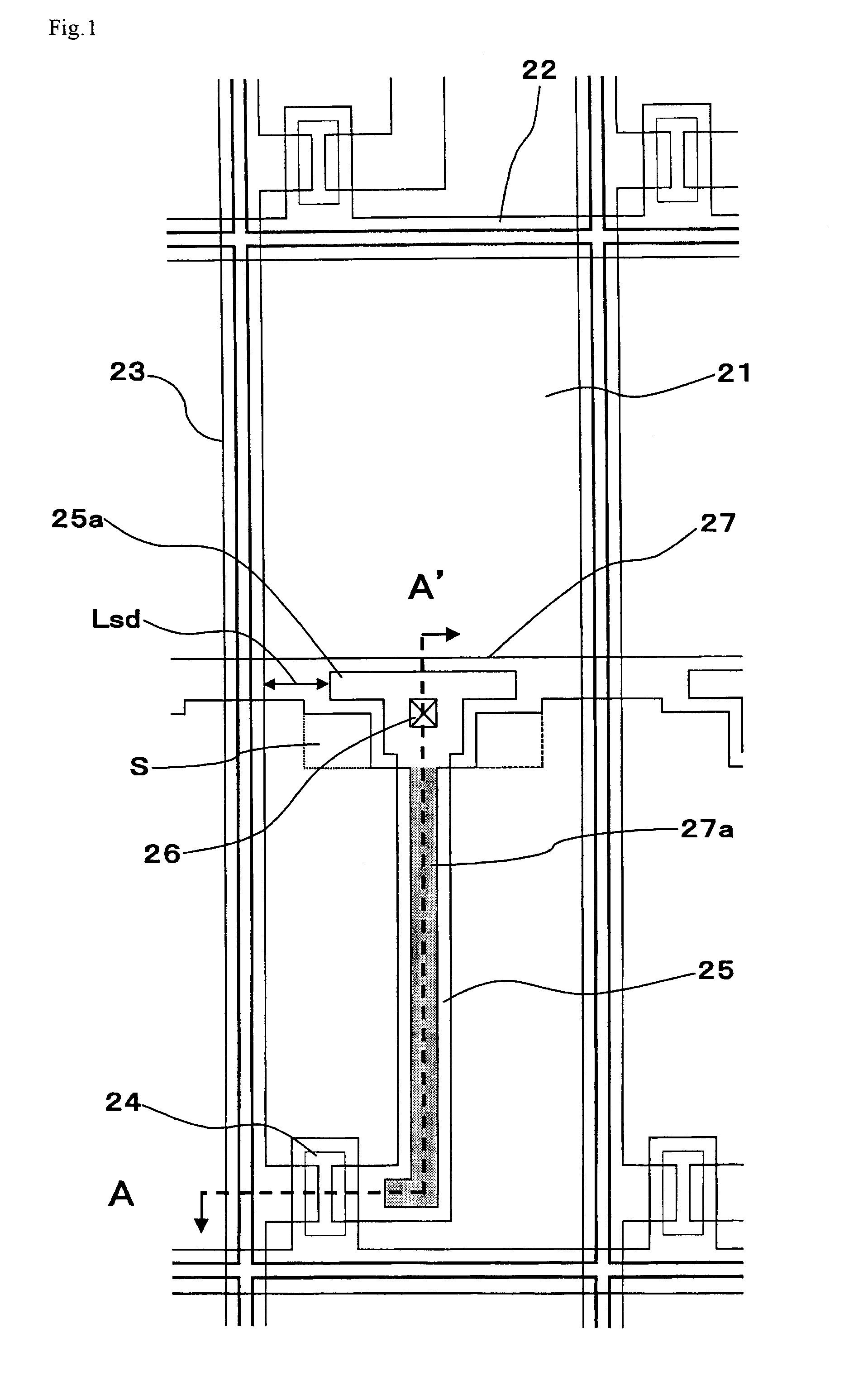
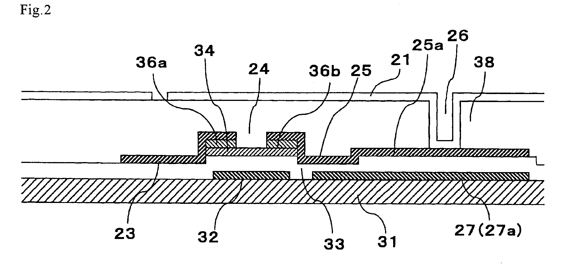
[0066]FIG. 1 is a planar view schematically showing a configuration of one pixel of an active matrix substrate according to Preferred Embodiment 1. FIG. 2 is a cross-sectional view schematically showing a cross-section of the active matrix substrate taken along line A-A′ in FIG. 1.

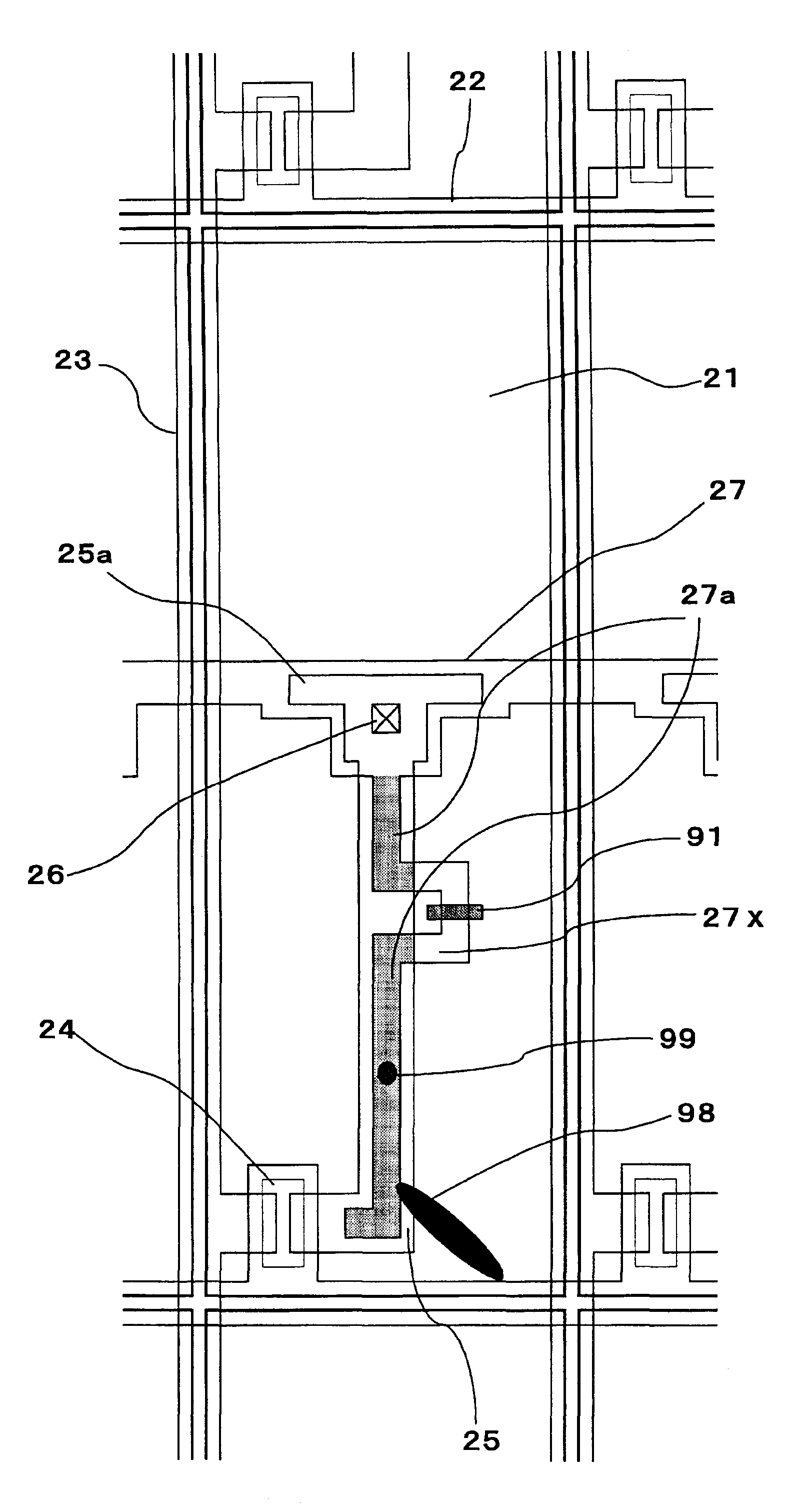
[0067]In FIG. 1, the active matrix substrate includes a plurality of pixel electrodes 21 arrayed in a matrix pattern. A scanning signal line 22 for supplying a scanning signal and a data signal line 23 for supplying a data signal are disposed to surround these pixel electrodes 22 and intersect with each other. At the intersection of the scanning signal line 22 and the data signal line 23, a TFT 24 as a switching element connected to the pixel electrode 21 is disposed. To a gate electrode 32 of this TFT 24, the scanning signal line 22 is connected, and the TFT 24 is driven and controlled by a scanning signal input into the gate electrode 32. The data signal line 23 is connected to a so...

embodiments 2 and 3

Preferred Embodiments 2 and 3

[0078]FIGS. 3 and 4 are planar views each schematically showing a configuration of one pixel of an active matrix substrate according to Preferred Embodiments 2 and 3, respectively.

[0079]In Preferred Embodiments 2 and 3, a separation region 27x not overlapping with the drain lead-out wiring 25 (hereinafter, also referred to as “non-overlapping portion”) is formed in the extending portion of the storage capacitor wiring 27a, as shown in FIGS. 3 and 4. In Preferred Embodiment 2, a bent portion of the extending portion of the storage capacitor wiring 27a having a substantially linear shape is the non-overlapping portion 27x. In Preferred Embodiment 3, a straight-line portion of the extending portion of the storage capacitor wiring 27a, which corresponds to the bent portion of the substantially linear drain lead-out wiring 25, is the non-overlapping portion 27x. Such a pattern including the non-overlapping portion 27x can be easily formed just by changing the...

embodiment 4

Preferred Embodiment 4

[0082]FIG. 5 is a planar view schematically showing a configuration of one pixel of an active matrix substrate according to Preferred Embodiment 4.

[0083]In the present Preferred Embodiment, the drain lead-out wiring 25 is formed to have a line width (Ld) smaller than a line width (Lcs′) of the extending portion of the storage capacitor wiring 27a, as shown in FIG. 5. Generally, the extending portion of the storage capacitor wiring 27a and the drain lead-out wiring 25 are pattern-formed by a photolithography method, and the drain lead-out wiring 25 is formed after the storage capacitor wiring 27 and the scanning signal line 22 are formed. However, a short circuit is easily generated at the end of the extending portion of the storage capacitor wiring 27a pattern because the presence of the step (taper) at the end reduces the coverage of the gate insulating film 33. For this problem, in the present Preferred Embodiment, the drain lead-out wiring 25 is formed to ha...


PUM

PropertyMeasurementUnit
widthaaaaaaaaaa
OFF-state currentaaaaaaaaaa
poweraaaaaaaaaa

Abstract

An active matrix substrate suppresses reduction in production yield and increase in production steps and simultaneously permits both sufficient securing of a storage capacity and improvement of an aperture ratio of a pixel. The active matrix substrate is an active matrix substrate and includes a thin film transistor disposed at an intersection of a scanning signal line with a data signal line on a substrate, the thin film transistor including a gate electrode connected to the scanning signal line, a source electrode connected to the data signal line, and a drain electrode connected to a drain lead-out wiring; a storage capacitor upper electrode connected to the drain lead-out wiring and a pixel electrode; and a storage capacitor wiring overlapping with the storage capacitor upper electrode through an insulating film, wherein the storage capacitor wiring has an extending portion overlapping with the drain lead-out wiring through the insulating film.

Description

BACKGROUND OF THE INVENTION[0001]1. Field of the Invention[0002]The present invention relates to an active matrix substrate and a display device. More specifically, the present invention relates to an active matrix substrate in which a thin film transistor for drive control of a liquid crystal layer and a storage capacitor element are disposed in every pixel, and also relates to an active matrix liquid crystal display device.[0003]2. Description of the Related Art[0004]Active matrix substrates have been widely used in active matrix display devices such as a liquid crystal display device and an EL (Electro luminescence) display device. In conventional active matrix liquid crystal display devices, a switching element such as a TFT (Thin Film Transistor) is disposed at every intersection of a plurality of scanning signal lines with a plurality of data signal lines disposed to intersect with each other on a substrate, and an image signal is transmitted to every pixel by a switching func...

Claims


Application Information

Patent Timeline
Patent Type & Authority Patents(United States)
IPC IPC(8): G02F1/1343G02F1/1333G02F1/1337
CPCG02F1/133707G02F1/136213G02F1/136227G02F1/136286
Inventor YAGI, TOSHIFUMITSUBATA, TOSHIHIDETOKUDA, TSUYOSHIENDA, KENJISHIMADA, YOSHINORIMARUOKA, SHINYA
Owner SHARP KK
Why Eureka
Try Eureka