Composite phase shifting lithography mask including etch stop layer

a phase shifting lithography and stop layer technology, applied in the field of semiconductor fabrication, can solve the problems of difficult control of the resulting parameters of the lithography mask fabrication etch process, inconvenient methods for fabricating lithography masks, and inability to accurately measure the thickness of light transmitting substrates, etc., to achieve the effect of reducing thickness

Active Publication Date: 2010-11-02
TEXAS INSTR INC
View PDF8 Cites 0 Cited by
  • Summary
  • Abstract
  • Description
  • Claims
  • Application Information

AI Technical Summary

Benefits of technology

[0010]The present invention relates to forming a lithography mask in a manner that allows select locations of the mask to be reduced in thickness by a specific amount. More particularly, a sandwich layer of etch stop material is included within the mask to halt the progression of an etching process so that an appropriate phase shift may be achieved by varying the etch depth into substrate material.

Problems solved by technology

However, conventional methods for fabricating lithography masks have several drawbacks.
For example, aside from the duration of an etching process and / or the chemistry of a homogeneous blanket film of the etching process, the precision of resulting parameters from lithography mask fabrication etch processes is difficult to control.
This can, for example, result in imprecise thicknesses of the light transmitting substrate.
Further, dry etching techniques are generally isotropic—meaning that they remove equal amounts of material in both horizontal and vertical directions.
This makes it difficult to form a deep yet narrow feature in a lithography mask, as may be desired to advance device scaling.
This reduces the ability to control critical dimensions independently of phase shift.

Method used


Image

  • Composite phase shifting lithography mask including etch stop layer
  • Composite phase shifting lithography mask including etch stop layer
  • Composite phase shifting lithography mask including etch stop layer

Examples


Embodiment Construction

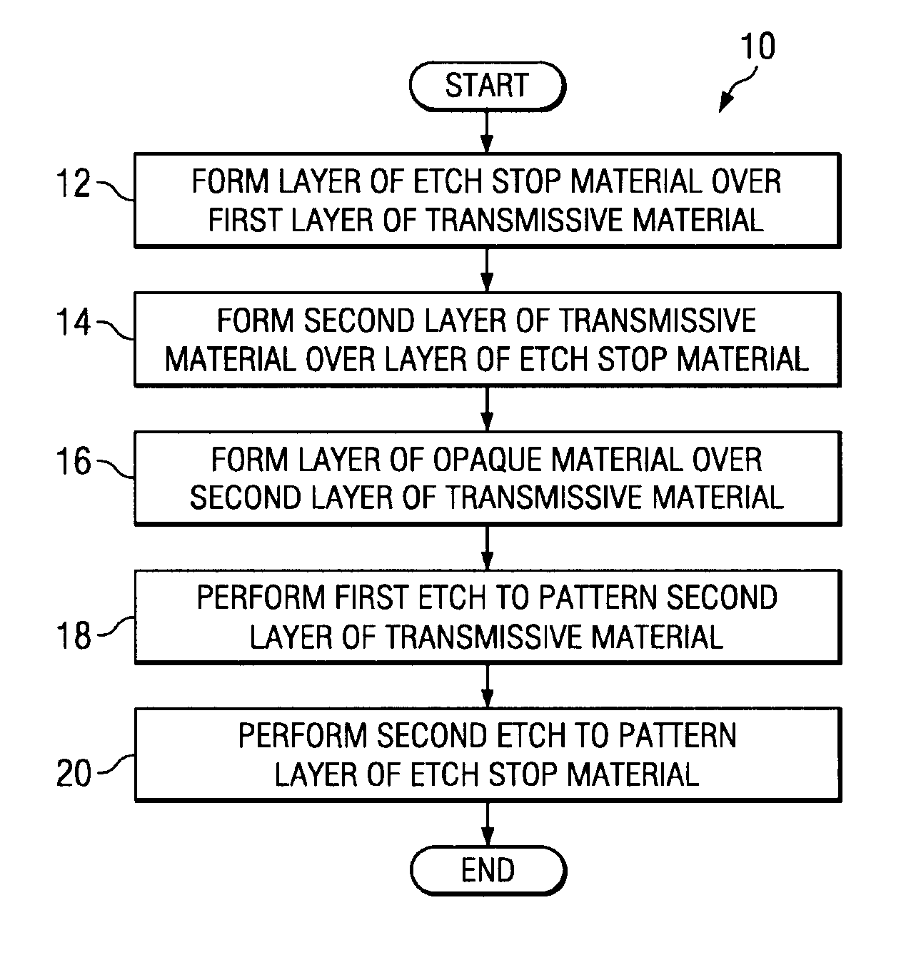
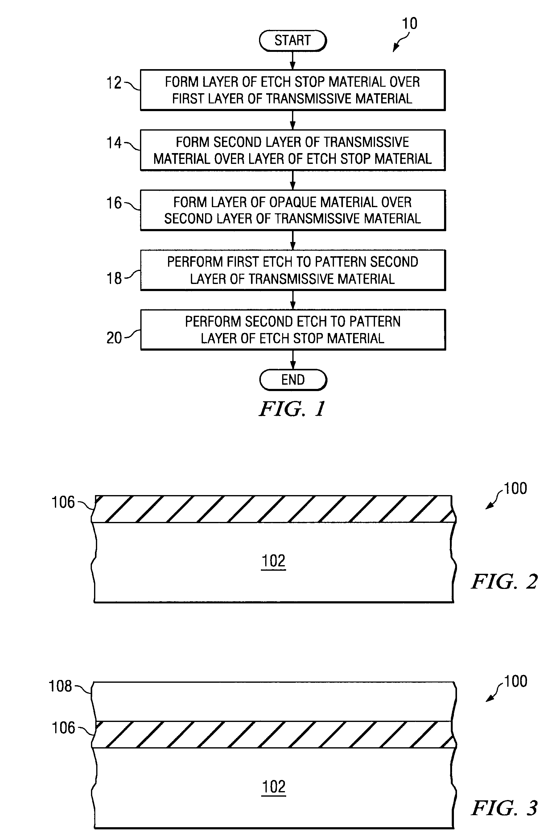
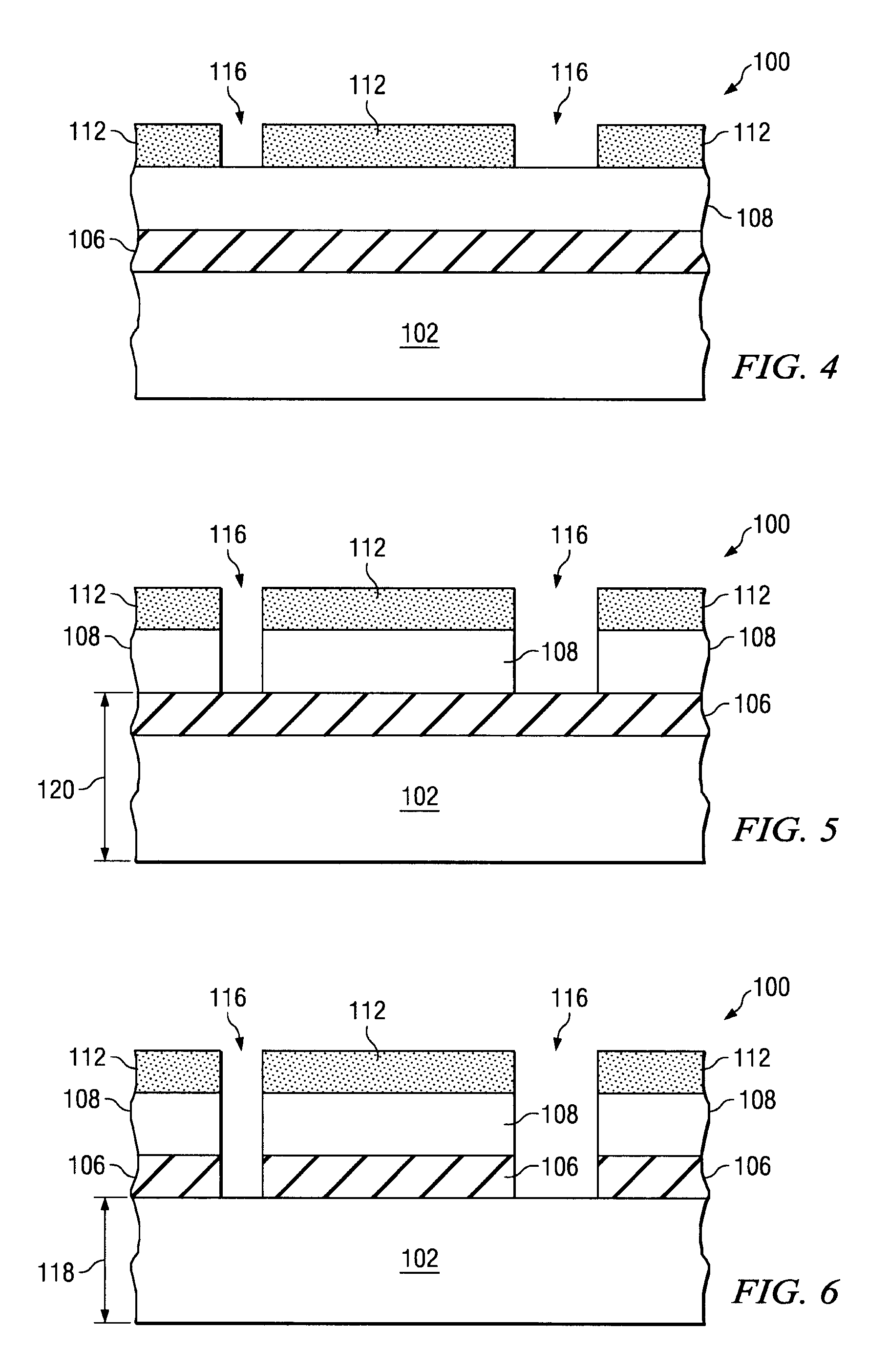
[0016]One or more aspects of the present invention are described with reference to the drawings, wherein like reference numerals are generally utilized to refer to like elements throughout, and wherein the various structures are not necessarily drawn to scale. It will be appreciated that where like acts, events, elements, layers, structures, etc. are reproduced, subsequent (redundant) discussions of the same may be omitted for the sake of brevity. In the following description, for purposes of explanation, numerous specific details are set forth in order to provide a thorough understanding of one or more aspects of the present invention. It may be evident, however, to one of ordinary skill in the art that one or more aspects of the present invention may be practiced with a lesser degree of these specific details. In other instances, known structures are shown in diagrammatic form in order to facilitate describing one or more aspects of the present invention.

[0017]Turning to FIG. 1, a...


PUM

PropertyMeasurementUnit
thicknessaaaaaaaaaa
thicknessaaaaaaaaaa
thicknessaaaaaaaaaa

Abstract

The formation of a lithographic mask (100) is disclosed, where the mask (100) can be used in forming integrated circuits onto a semiconductor substrate. A layer of etch stop material (106) is sandwiched between first (102) and second (108) layers of transmissive material that are substantially transparent to lithographic light. The layer of etch stop material (106) serves as an etch stop when a circuit pattern is etched into the second layer of transmissive material (108). This allows the second layer of etch stop material (108) to be etched to a more precise depth thereby providing a desired phase shift and concurrently controlling critical dimension width.

Description

FIELD OF INVENTION[0001]The present invention relates generally to semiconductor fabrication, and more particularly to forming a lithography mask that can be used in patterning a semiconductor substrate.BACKGROUND OF THE INVENTION[0002]It can be appreciated that several trends presently exist in the electronics industry. Devices are continually getting smaller, faster and requiring less power, while simultaneously being able to support and perform a greater number of increasingly complex and sophisticated functions. One reason for these trends is an ever increasing demand for small, portable and multifunctional electronic devices. For example, cellular phones, personal computing devices, and personal sound systems are devices which are in great demand in the consumer market. These devices rely on one or more small batteries as a power source while providing increased computational speed and storage capacity to store and process data, such as digital audio, digital video, contact inf...

Claims


Application Information

Patent Timeline
Patent Type & Authority Patents(United States)
IPC IPC(8): G03F1/00
CPCG03F1/26G03F1/32G03F1/08G03F1/80
Inventor PAS, SYLVIA
Owner TEXAS INSTR INC
Why Eureka
Try Eureka