U-shaped SONOS memory having an elevated source and drain

a sonos memory and source technology, applied in the field of u-shaped sonos memory with an elevated source and drain, can solve the problems of difficult structure to miniaturize the memory cell, the p-type density of the semiconductor substrate cannot be increased, and the difficulty of flash memory having this structure, etc., to achieve the effect of suppressing the channel length and miniaturizing the memory cell

Active Publication Date: 2010-11-02
MONTEREY RES LLC
View PDF3 Cites 0 Cited by
  • Summary
  • Abstract
  • Description
  • Claims
  • Application Information

AI Technical Summary

Benefits of technology

[0008]According to an aspect of the present invention, there is provided a semiconductor device which includes two epitaxial semiconductor layers formed on a semiconductor substrate, bit lines formed on upper portions of the two epitaxial semiconductor layers, and a charge storage layer formed on the semiconductor substrate between the two epitaxial semiconductor layers. In the present invention, as the width of the bit line is substantially defined by the width of the epitaxial semiconductor layer, reduction in the channel length can be suppressed. This makes it possible to miniaturize the memory cell.
[0009]In one embodiment, a groove may be formed in the semiconductor substrate between the two epitaxial semiconductor layers, and the charge storage layer may be formed along an inner surface of the groove. This structure can suppress fluctuation of the channel length due to variation in the depth of the groove. Accordingly, it is possible to maintain the channel length while miniaturizing the memory cell. In a further embodiment, each of the two epitaxial semiconductor layers may be entirely formed as a bit line. Furthermore, the charge storage layer may also be formed on each side of the two epitaxial semiconductor layers.
[0010]According to another aspect of the present invention, there is provided a method for manufacturing a semiconductor device comprising: forming a charge storage layer on a region of a semiconductor substrate corresponding to an area between two epitaxial semiconductor layers, forming the two epitaxial semiconductor layers on the semiconductor substrate, and forming a bit line on each upper portion inside the two epitaxial semiconductor layers. In the method, because the bit line width is substantially defined by the width of the epitaxial semiconductor layer, the reduction in the channel length can be suppressed. Accordingly, it is possible to miniaturize the memory cell.
[0012]In a further embodiment, the two epitaxial semiconductor layers may be formed using the charge storage layer as a mask to simplify the manufacturing step.
[0013]In a still further embodiment, the method for manufacturing a semiconductor device may further comprise forming a mask layer on a region corresponding to the area between the two epitaxial semiconductor layers. In this embodiment, forming the two epitaxial semiconductor layers, the two epitaxial semiconductor layers may be formed, for example, by using the mask layer as a mask. In a further embodiment, the two epitaxial semiconductor layers may be formed to have one or more upper surfaces lower than that of the mask layer. Accordingly, this method allows the angle of the side surface of the epitaxial semiconductor layer to be defined to a desired value.
[0015]According to the present invention, because the width of the bit line is substantially defined by the width of the epitaxial semiconductor layer, reduction in the channel length can be suppressed. This makes it possible to miniaturize the memory cell.

Problems solved by technology

As a result, it is difficult for flash memory having this structure to miniaturize the memory cell while keeping the channel length.
Accordingly, this structure has difficulties in miniaturization of the memory cell.
Furthermore, because the bit line is formed inside the semiconductor substrate, a p-type density of the semiconductor substrate cannot be increased.

Method used


Image

  • U-shaped SONOS memory having an elevated source and drain
  • U-shaped SONOS memory having an elevated source and drain
  • U-shaped SONOS memory having an elevated source and drain

Examples


third embodiment

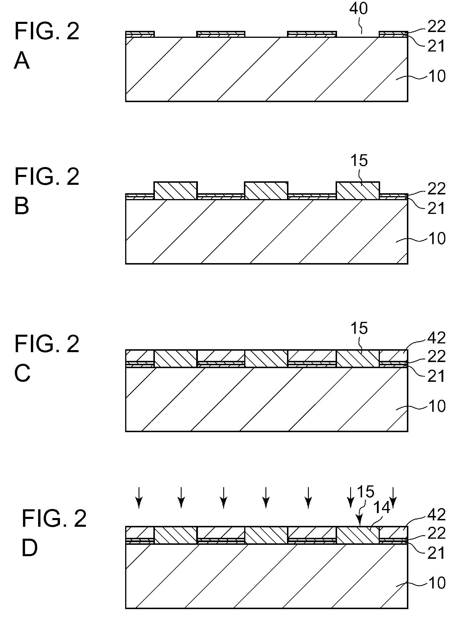
[0055]Pocket implantation using boron and the like may be performed for the region of the semiconductor substrate 10 corresponding to the area between the epitaxial semiconductor layers to form a p-type pocket implantation region 18 as shown in FIG. 11A. Referring to FIG. 11B, the epitaxial semiconductor layer 15 is epitaxially grown on the semiconductor substrate 10. Thereafter, the steps subsequent to the step shown in FIG. 7A are performed to produce a flash memory according to this embodiment.

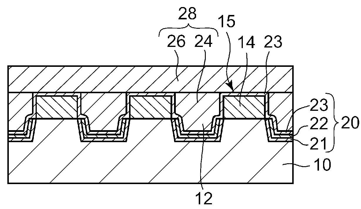
[0056]The pocket implantation region 18 is formed between the channel and the bit line 14 in contact with the bit line 14 as a doped p-type region higher than the channel (semiconductor substrate 10). This makes it possible to increase the electric field in the region between the channel and the bit line 14 so as to improve the property for writing and deleting the charge into or from the trap layer 22.

[0057]In another embodiment, the pocket implantation region is formed adjacent to the gr...

eighth embodiment

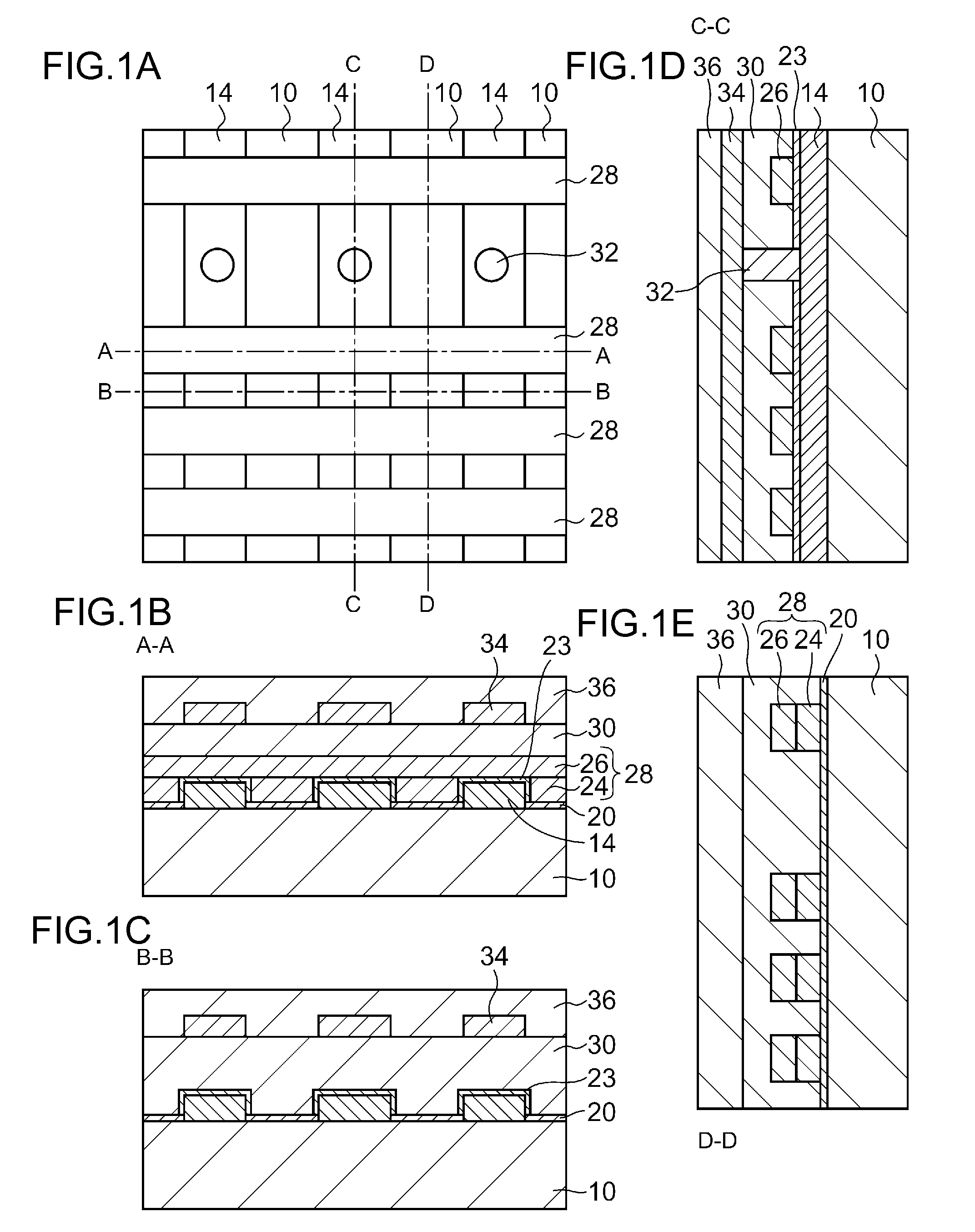
[0060]Referring to FIG. 15A, the lower mask layer 54 is eliminated. Then, the ONO film 20 is formed to coat the upper surface of the semiconductor substrate 10 and the epitaxial semiconductor layer 15. Referring to FIG. 15B, the word line 28 formed of the first and the second polysilicon layers 24 and 26 is formed. Thereafter, an interlayer insulation film, a plug electrode, a wiring layer and a protection film are formed to produce a flash memory according to the

[0061]According to one embodiment, the ONO film 20 is formed also on the sides of the epitaxial semiconductor layer 15 as shown in FIG. 15A. The side portion of the epitaxial semiconductor layer 15 and the upper surface of the semiconductor substrate 10 may form a channel without forming a groove in the semiconductor substrate 10. This can further improve controllability of the channel length.

[0062]Referring to FIG. 14A, the lower mask layer 54 and the polish stopper layer 56 are formed as the mask layer 58. Thus, as shown ...


PUM


Abstract

A semiconductor device and a method for manufacturing thereof are provided. The semiconductor device includes two epitaxial semiconductor layers formed on a semiconductor substrate, bit lines formed on upper portions of the two epitaxial semiconductor layers, and a charge storage layer formed on the semiconductor substrate between the two epitaxial semiconductor layers.

Description

CLAIM OF PRIORITY[0001]This application claims priority from Japanese patent application 2007-213000 filed on Aug. 17, 2007.TECHNICAL FIELD[0002]The invention relates to a semiconductor device and a method for manufacturing thereof. More particularly, this invention relates to a semiconductor device having a bit line formed of a semiconductor epitaxially grown and a method for manufacturing thereof.BACKGROUND OF THE INVENTION[0003]Recently, the usage of non-volatile memory comprising a semiconductor device capable of rewriting data and retaining data stored therein even while the device is un-powered has become increasingly popular. Flash memory is one example of non-volatile memory. A typical flash memory is provided with a transistor which operates as a memory cell and includes a floating gate or an insulating film called a charge storage layer for accumulating electrons used to store data. Flash memory with a SONOS (Silicon Oxide Nitride Oxide Silicon) structure for accumulating ...

Claims


Application Information

Patent Timeline
Patent Type & Authority Patents(United States)
IPC IPC(8): H01L27/108
CPCH01L27/11568H01L29/66833H01L29/792H10B43/30
Inventor OKANISHI, MASATOMIMIKASA, YOSHIHIROMURAI, HIROSHI
Owner MONTEREY RES LLC
Why Eureka
Try Eureka