

Semiconductor device and method for fabricating the same
a technology of semiconductors and polysilicon films, applied in the direction of semiconductor devices, electrical equipment, transistors, etc., can solve the problems of difficult to prevent the interdiffusing of impurities in the polysilicon film, the threshold voltage of transistors is variable, and the intended characteristics cannot be obtained, etc., to achieve the effect of suppressing the threshold voltage variation
- Summary
- Abstract
- Description
- Claims
- Application Information
AI Technical Summary
Benefits of technology
Problems solved by technology
Method used
Image

Examples
first embodiment
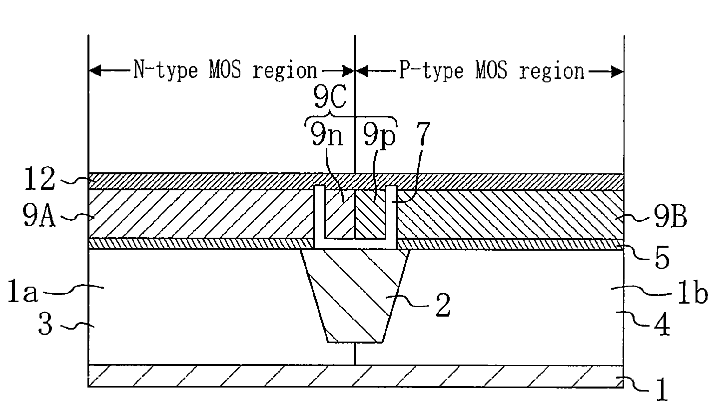
[0023]Hereinafter, a semiconductor device and a method for fabricating the semiconductor device according to a first embodiment of the invention will be described with reference to the accompanying drawings. FIG. 1 is a cross-sectional view in a gate-width direction, illustrating the structure of the semiconductor device according to the first embodiment of the invention. A MOSFET having a dual-gate electrode will be described as the inventive semiconductor device.
[0024]As shown in FIG. 1, the semiconductor device according to this embodiment includes a semiconductor substrate 1 made of silicon or the like; an isolation region 2 formed in the semiconductor substrate 1 by an STI (Shallow Trench Isolation) technique or the like; a p-type well 3 formed in an n-type MOS region in the semiconductor substrate 1; an n-type well 4 formed in a p-type MOS region in the semiconductor substrate 1; a first active region 1a surrounded by the isolation region 2 in the semiconductor substrate 1 (th...
second embodiment
[0039]Hereinafter, a semiconductor device and a method for fabricating the semiconductor device according to a second embodiment of the invention will be described with reference to the accompanying drawings. FIG. 4 is a cross-sectional view illustrating the structure of the semiconductor device according to this embodiment.
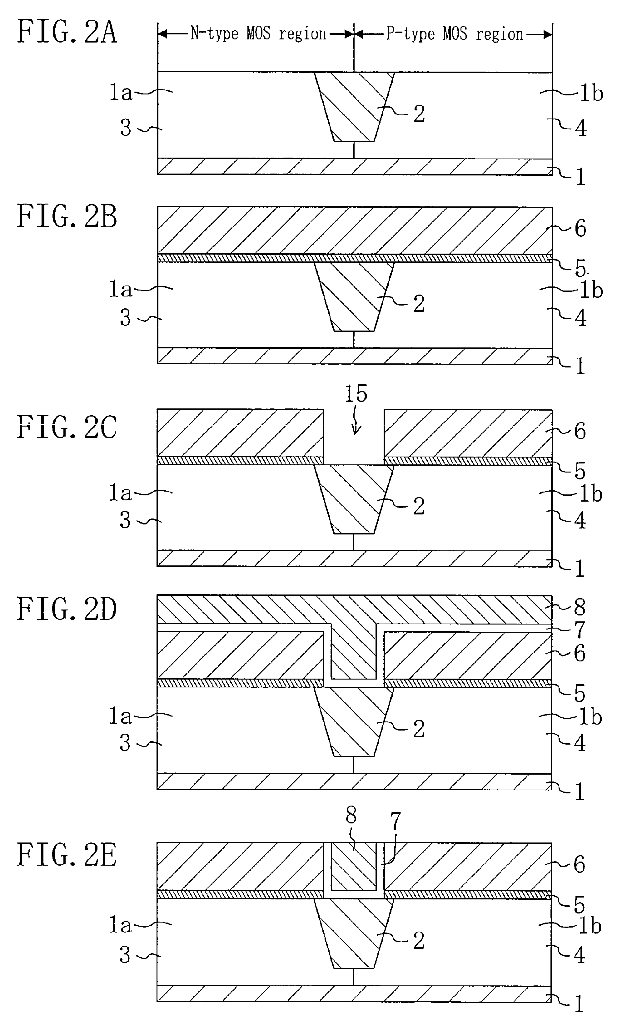
[0040]As shown in FIG. 2C, in the above-described semiconductor device according to the first embodiment, the opening 15 provided between the n-type gate electrode 9A and the p-type gate electrode 9B is formed so that the side faces of the n-type gate electrode 9A and p-type gate electrode 9B are almost perpendicular to the isolation region 2. Thus, the insulating film 7 is formed to have the shape of a recess in which the lateral regions thereof are substantially perpendicular to the bottom region. In contrast, as shown in FIG. 4, in the semiconductor device according to this embodiment, an opening 15A provided between an n-type gate electrode 9A and a p-type ga...
third embodiment
[0044]Hereinafter, a semiconductor device and a method for fabricating the semiconductor device according to a third embodiment of the invention will be described with reference to the accompanying drawings. FIG. 5 is a cross-sectional view illustrating the structure of the semiconductor device according to this embodiment.
[0045]As shown in FIG. 1, in the above-described semiconductor device of the first embodiment, the n-type gate electrode 9A and the p-type gate electrode 9B are separated by the insulating film 7 and the silicon region9C. In contrast, in the semiconductor device according to this embodiment, an n-type gate electrode 9A and a p-type gate electrode 9B are separated by an insulating film 14 alone, as shown in FIG. 5.
[0046]Specifically, the semiconductor device according to this embodiment includes: a semiconductor substrate 1, in which an isolation region 2, a p-type well 3, an n-type well 4, a first active region 1a, and a second first active region 1b are formed; a...
PUM
 Abstract
Description
Claims
Application Information