Semiconductor device with ion movement control

a technology of ion movement and semiconductor devices, applied in semiconductor devices, digital storage, instruments, etc., can solve problems such as uneven diffusion of metal ions, electrolytic layer, and unstable rewriting characteristics

Inactive Publication Date: 2010-11-09
HITACHI LTD
View PDF3 Cites 10 Cited by
  • Summary
  • Abstract
  • Description
  • Claims
  • Application Information

AI Technical Summary

Benefits of technology

[0005]Concretely, in case of a metal-chalcogenide or metal-oxide solid electrolyte memory in which chalcogenide or oxide is used to form a solid electrolytic layer to be disposed between a pair of electrodes, ions move in accordance with the memory mechanism and a low resistance conductive path is formed in the chalcogenide layer or oxide layer to realize a non-volatile memory. The conductive path contains highly concentrated plus ions of such an element as Ag, Cu, or the like. And when those ions are return toward the original electrode with a backward voltage, the conductive path restores its high resistance state, thereby enabling information rewriting in the memory.
[0006]If such information rewriting is repeated in the memory, however, metal ions are diffused unevenly in the solid electrolytic layer from the metal electrodes. As a result, the shape of the surface of the electrodes comes to change on the atomic level, causing the rewriting characteristics to become unstable, thereby the resistance might change at each rewriting time. Furthermore, while rewriting is repeated, the Ag and Cu come to be concentrated excessively due to their diffusion from the electrodes, thereby the surface shapes of the electrodes might not change with the resistance between ON and OFF states. Although the high resistance state (OFF) can also be set with a high voltage / current that might generate a heat in some cases even when the voltage direction is the same as the resistance lowering one, the metal ion concentration in the solid electrolyte is further quickened by the repetitive rewriting. The rewriting endurance is thus more lowered. In addition, the resistance of the conductive path easily varies among memory elements. Consequently, those causes come to degrade the performance of the subject information recordable semiconductor device and it will become difficult to realize larger capacity and higher integration in memories by multi-value / multi-bit recording techniques.
[0007]Under such circumstances, it is an object of the present invention to provide a technique that enables coexistence of both logic elements and memory elements in a highly integrated recordable semiconductor device. The semiconductor device is structured so as to control movements of ions in the solid electrolyte very precisely, thereby improving its performance. The semiconductor device is required to have just one layer for transistors or diodes even when it is structured as a multilayered three-dimensional one or required to have only diodes at points of X-Y intersection in the array on each layer, so that the high integration comes to be realized at a low cost.
[0012]In order to realize a difference of the mobility among elements that contribute to the forming of a conductive path in such a way, the present inventor has had a notation of making a difference among the gaps of atomic arrays through which an element useful to form such a conductive path, as well as a difference of the attracting and coupling forces between an element useful to form the conductive path and an element used to form a recording layer. The solid electrolytic layer often contains elements of six groups. And because the radius of atoms and ions becomes larger in the order of oxygen, sulfur, selenium, and tellurium that are listed up vertically in the periodic law table, metal ions can pass easily among any of those elements, that is, the mobility of metal ions becomes higher. In this case, it is premised that the elements of the six groups couple with the same element. In case of a nitride that contains elements of five groups, the mobility is considered to be approximately the same as that in oxide.
[0039]In the semiconductor device, two or more layers having different components respectively are formed between a pair of electrodes disposed separately in the vertical direction (Z-axis direction) and a pulse voltage is applied between those electrodes to form a conductive path. The conductive path is assumed as a semiconductor element capable of changing its resistance value according to information to be recorded. Furthermore, a region that accumulates a conductivity improving component is formed in the middle of the conductive path, thereby relating the resistivity of the conductive path to an information signal correctly. And preferably, an electrode should be formed at least in either the X-axis or Y-axis direction and a control voltage should be applied to the electrode. Consequently, ions diffused from the upper electrode are returned moderately toward the upper electrode, thereby the element on / off operations can be repeated many times stably with the voltage in the same direction (the Z-axis direction). As a result, instead of a transistor, a diode can be formed at each point of X-Y intersection of the subject memory array and the memory array can be driven at a low cost. This technique can also apply to multi-value recording correctly. The resistance between the upper electrode in the Z-axis direction and an X-axis direction electrode, as well as an electromotive force generated by electromagnetic induction may also be used to read data. Employment of a three-dimensional matrix also enables multi-bit recording. At least part of the above-described conductive path may also be related to an information signal to be formed with an angle from the direction connecting a pair of electrodes and furthermore, the conductive path may be switched over to, branched to, and jointed into another.

Problems solved by technology

If such information rewriting is repeated in the memory, however, metal ions are diffused unevenly in the solid electrolytic layer from the metal electrodes.
As a result, the shape of the surface of the electrodes comes to change on the atomic level, causing the rewriting characteristics to become unstable, thereby the resistance might change at each rewriting time.
Consequently, those causes come to degrade the performance of the subject information recordable semiconductor device and it will become difficult to realize larger capacity and higher integration in memories by multi-value / multi-bit recording techniques.

Method used


Image

  • Semiconductor device with ion movement control
  • Semiconductor device with ion movement control
  • Semiconductor device with ion movement control

Examples


first embodiment

[0068]In this first embodiment, the semiconductor device includes a memory elements, and the material and structure employed for the memory elements are the main features of the present invention.

(Basic Structure of the Memory Element)

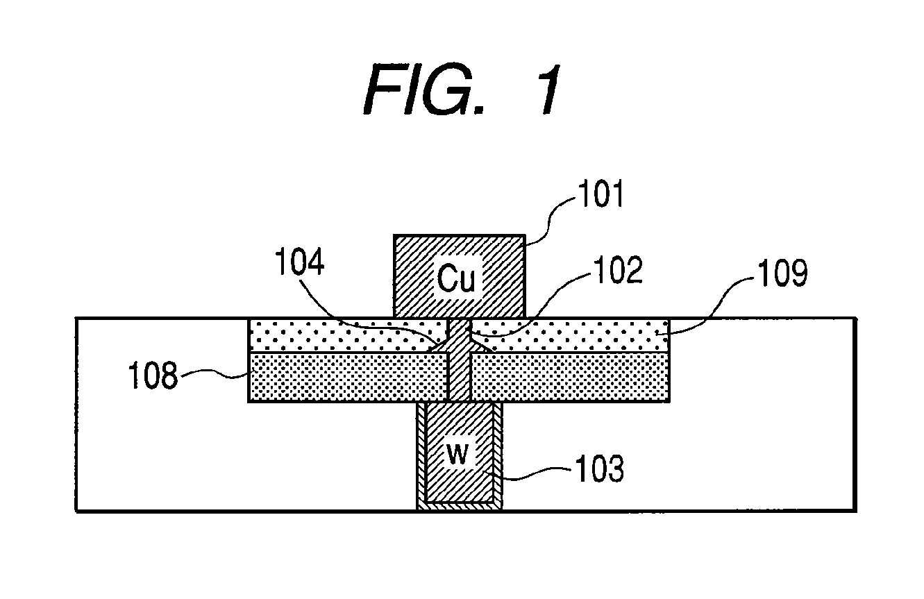
[0069]FIG. 1 shows a cross sectional view of the basic structure of a memory element in this first embodiment. The memory element includes a lower electrode 103 formed on a semiconductor substrate; an upper electrode 101 formed on the semiconductor substrate; two layers (solid electrolytic layers 108 and 109) formed on the semiconductor substrate between the upper and lower electrodes 101 and 103. Furthermore, a conductive path is formed in a solid electrolytic layer on a path connecting the upper and lower electrodes to each other and a conductive material accumulating region 104 is formed near the phase boundary between the two solid electrolytic layers.

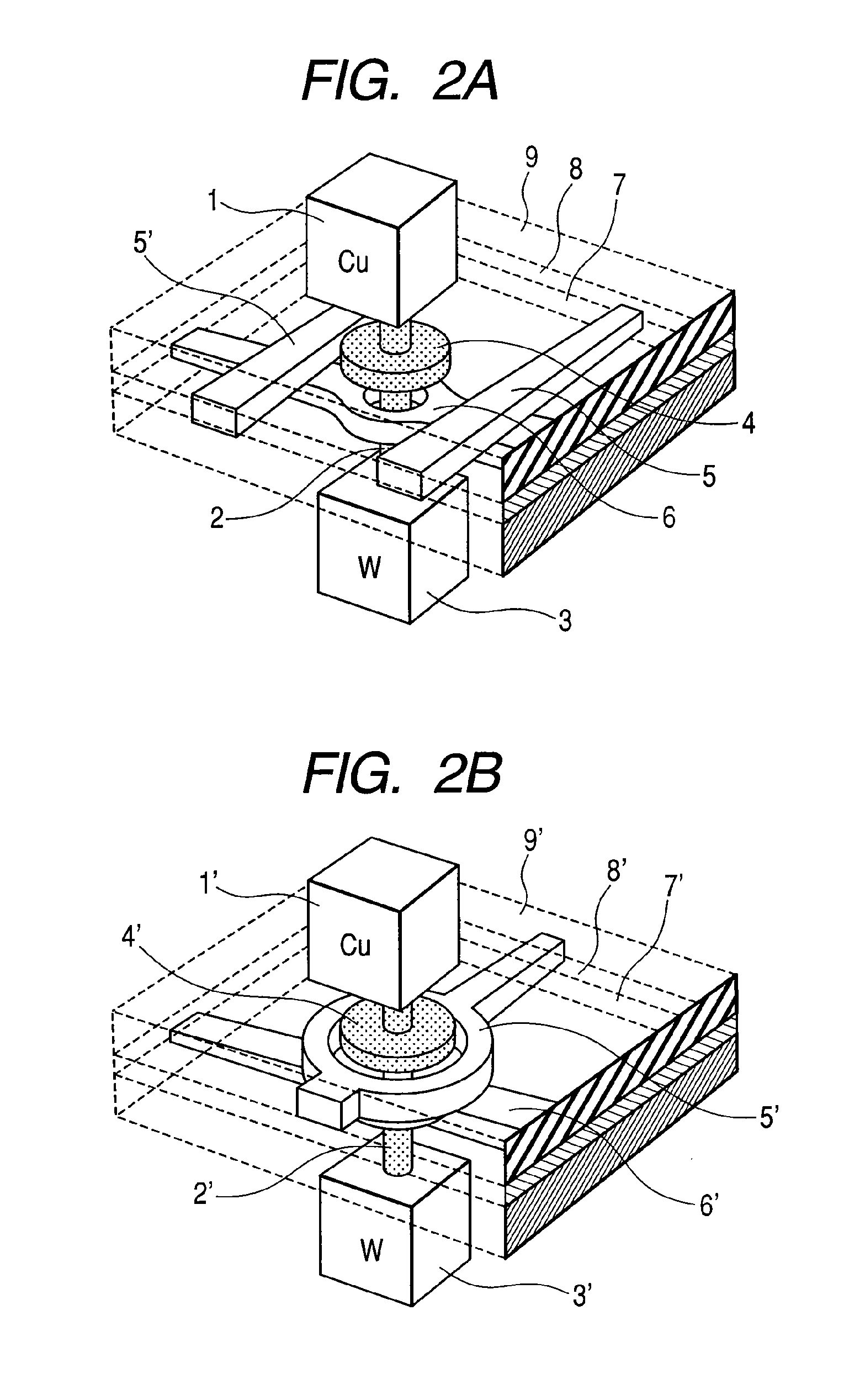
[0070]FIG. 2 shows a bird's-eye view of the memory element in this first embodiment. The memory el...

second embodiment

(Three-Dimensional Matrix Structure)

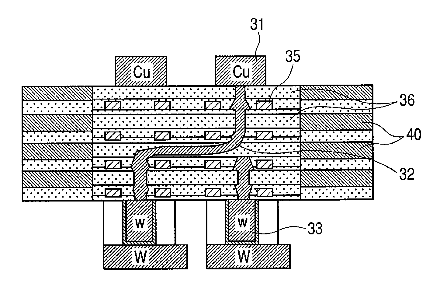
[0152]In this second embodiment, multiple layers having different components respectively are deposited between a pair of electrodes and a high conductivity path is formed with a voltage applied between those electrodes. Information is recorded in each object memory cell by changing the resistance value between the above pair of electrodes or between other electrodes that are disposed orthogonal to the above paired electrodes.

[0153]In this second embodiment, a region for accumulating a conductivity improving component is formed in the middle of the high conductivity path.

[0154]In this second embodiment, there are a plurality of regions for accumulating a conductivity improving component respectively between a pair of electrodes.

[0155]Each region for accumulating a conductivity improving component corresponds to recorded information.

[0156]At each phase boundary described above is formed a small lump of element used to form a high conductivity path ...

third embodiment

[0171]In this third embodiment, at least part of the high conductivity path described above is formed with an angle from a direction connecting two electrodes to each other.

[0172]There should preferably be provided a plurality of regions for accumulating a conductivity improving component respectively or a plurality of portions formed so as to have an angle from a direction connecting the two electrodes between a pair of electrodes.

[0173]In case of a typical structure in this third embodiment, as shown in FIG. 21, electrodes 50 and 50′ are provided to apply a voltage in a direction having an angle from the direction connecting the two electrodes to each other. This means that two parallel electrodes that pass through each layer are provided for each of the above paths in parallel to a high conductivity path.

[0174]In this third embodiment, a phase boundary between a direction of a high conductivity path, which connects two electrodes to each other and a portion having an angle from t...


PUM


Abstract

A technique that can realize high integration even for multilayered three-dimensional structures at low costs by improving the performance of the semiconductor device having recording or switching functions by employing a device structure that enables high precision controlling of the movement of ions in the solid electrolyte. The semiconductor element of the device is formed as follows; two or more layers are deposited with different components respectively between a pair of electrodes disposed separately in the vertical (z-axis) direction, then a pulse voltage is applied between those electrodes to form a conductive path. The resistance value of the path changes according to an information signal. Furthermore, a region is formed at a middle part of the conductive path. The region is used to accumulate a component that improves the conductivity of the path, thereby enabling the resistance value (rate) to response currently to the information signal. More preferably, an electrode should also be formed at least in either the x-axis or y-axis direction to apply a control voltage to the electrode.

Description

CLAIM OF PRIORITY[0001]The present application claims priority from Japanese patent application JP 2007-183409 filed on Jul. 12, 2007, the content of which is hereby incorporated by reference into this application.FIELD OF THE INVENTION[0002]The present invention relates to a semiconductor device, more particularly to a technique to be applied effectively to semiconductor devices provided with a memory element respectively.BACKGROUND OF THE INVENTION[0003]There are some types of well-known non-volatile memories referred to as RRPMs, ReRAMs, solid electrolyte memories, or polarized memories (e.g., refer to JP-A 2006-173267, T. Sakamoto et al “IEEE International Solid-State Circuits Conference (ISSCC) 2004”, Digest, (issued in USA), 2004, p 16.3, and M. N. Kozicki et al “Proc. Non-Volatile Memory Technology Symposium (MVMTS) 2004)”, (issued in USA), 2004, pp. 10 to 17). In most of those non-volatile memories, each item of information is written therein according to a change of the res...

Claims


Application Information

Patent Timeline
Patent Type & Authority Patents(United States)
IPC IPC(8): H01L27/108
CPCG11C11/5614G11C13/0011H01L27/2409H01L27/2436H01L27/2463H01L27/2481H01L45/085H01L45/1233H01L45/1266H01L45/142H01L45/143H01L45/144H01L45/145H01L45/146G11C2213/11G11C2213/79H10B63/20H10B63/30H10B63/80H10B63/84H10N70/245H10N70/8416H10N70/826H10N70/8822H10N70/8825H10N70/8828H10N70/8833H10N70/883H01L27/10
Inventor TERAO, MOTOYASUMATSUOKA, HIDEYUKIIRIE, NAOHIKOSASAGO, YOSHITAKATAKEMURA, RIICHIROTAKAURA, NORIKATSU
Owner HITACHI LTD
Why Eureka
Try Eureka