

Low side N-channel FET protection circuit
a protection circuit and low-side technology, applied in the direction of safety/protection circuits, instruments, material electrochemical variables, etc., can solve the problems of increasing cost, excessive charge, and most batteries generating hea
- Summary
- Abstract
- Description
- Claims
- Application Information
AI Technical Summary
Benefits of technology
Problems solved by technology
Method used
Image

Examples
first embodiment
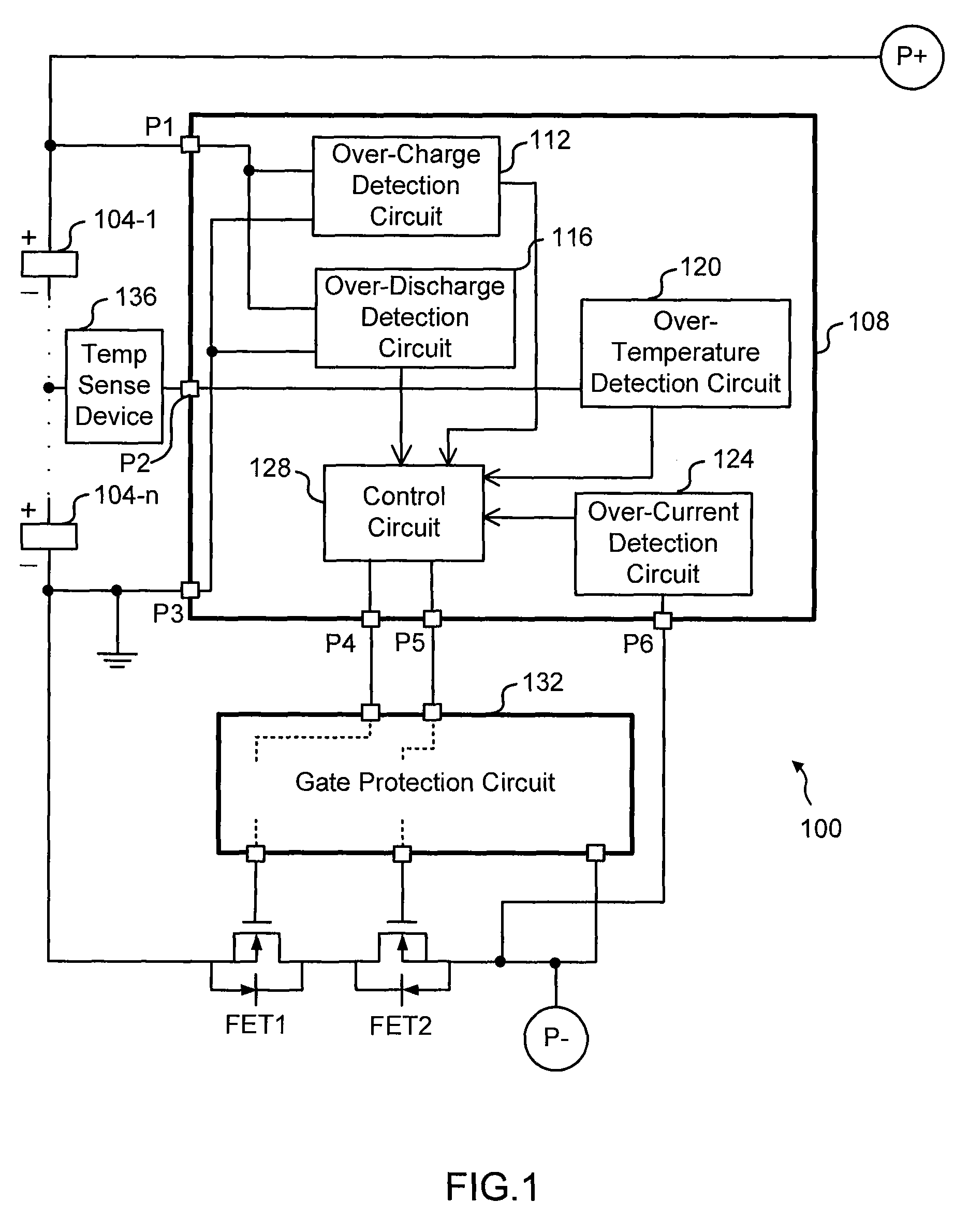
[0017]FIG. 1 is a block diagram showing a battery protection circuit 100 coupled to a plurality of batteries 104-1 through 104-n connected in series. P+ denotes a positive terminal, which is a connection point to an external device at the positive side of the battery pack; and P− denotes a negative terminal, which is a connection point to the external device at the negative side of the battery pack. When the batteries need to be recharged, a charger is attached to P+ and P−, and the charge current flows from P+ through the battery pack to P−. When a load is attached to P+ and P−, the battery pack sources energy to the load, and the discharge current flows from P+ through the load to P−. A controller 108 comprises an over-charge detection circuit 112, an over-discharge detection circuit 116, an over-temperature detection circuit 120, an over-current detection circuit 124 and a control circuit 128, and outputs control signals for controlling ON / OFF of the two N-channel MOSFETs (FET1 ...
second embodiment
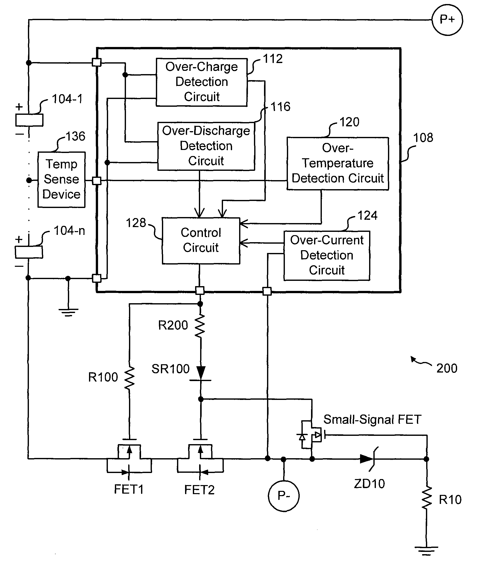
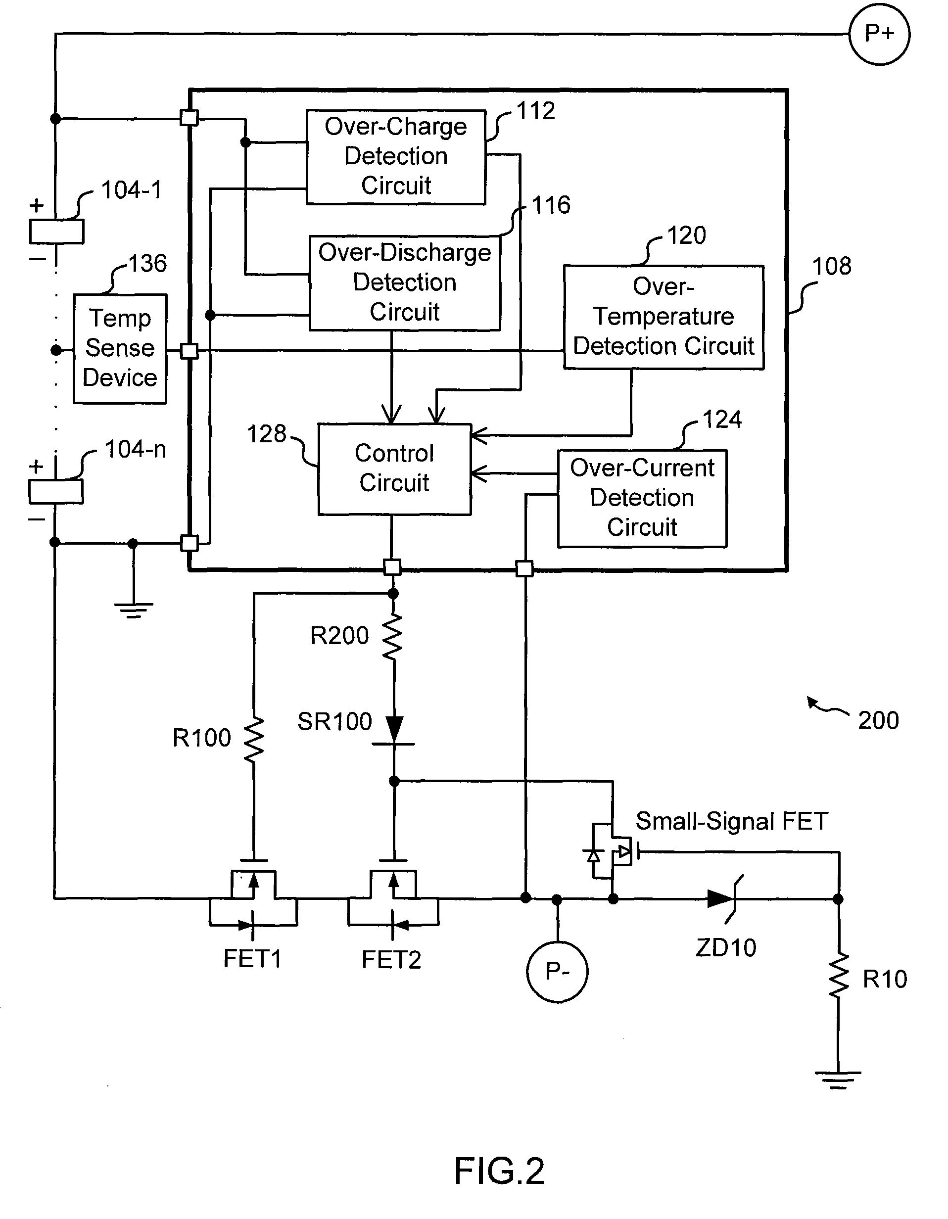
[0024]FIG. 2 is a block diagram showing a protection circuit 200 according to the present invention. A specific implementation of the gate protection circuit 132 is depicted. In this embodiment, the gate protection circuit 132 comprises three resistors R10, R100 and R200, one Schottky diode SR100, one Zener diode ZD10, and one small-signal FET. The resistor R10 is connected to the second ground. P− is connected to a point internal to the point where the small-signal FET is connected. The gates of FET1 and FET2 are coupled to the common output pin of the controller 108, receiving a control signal from the control circuit 128. Thus, ON / OFF of FET1 and FET2 is controlled by the same control signal from the single output pin in this embodiment. In another embodiment, the circuit is configured such that the two gates receive separate control signals from respective output pins to separately control ON / OFF of the two MOSFETs.
[0025]The voltage at the output pin (i.e. the output voltage of ...
fourth embodiment
[0035]FIG. 6 is a block diagram showing a battery protection circuit 600 according to the present invention. In this embodiment, the gate protection circuit 132 is integrated with various detection and control circuits on a same chip to provide a control IC 608. Thus, the battery protection circuit 600 comprises two discrete power MOSFETs (FET1 and FET2) and the control IC 608, resulting in reduced parts count.
PUM
| Property | Measurement | Unit |
|---|---|---|
| total voltage | aaaaa | aaaaa |
| energy density | aaaaa | aaaaa |
| voltage | aaaaa | aaaaa |
Abstract
Description
Claims
Application Information