Substrate supporting structure for semiconductor processing, and plasma processing device

a supporting structure and semiconductor technology, applied in the direction of chucks, manufacturing tools, mechanical equipment, etc., can solve the problems of increasing the footprint of the semiconductor processing device, reducing the productivity of the semiconductor device, and incurred substantial cost increases, so as to reduce the cost

Inactive Publication Date: 2010-11-23
TOKYO ELECTRON LTD
View PDF32 Cites 188 Cited by
  • Summary
  • Abstract
  • Description
  • Claims
  • Application Information

AI Technical Summary

Benefits of technology

[0005]It is, therefore, an object of the present invention to provide a substrate supporting structure and a plasma processing device for semiconductor processing capable of realizing a scaling-down for miniaturization and reducing cost.
[0006]It is another object of the present invention to provide a plasma processing device capable of increasing at least inter-surface uniformity of a film formed on a substrate to be processed.

Problems solved by technology

Thus, the footprint of the semiconductor processing device is increased, and the number of devices, which can be disposed in a semiconductor production factory, is accordingly decreased to thereby lower the productivity of the semiconductor device.
Further, if components for a 200 mm substrate are scaled up to be used for a 300 mm substrate while employing the conventional substrate supporting structure as it is, a substantial cost increase is incurred.

Method used


Image

  • Substrate supporting structure for semiconductor processing, and plasma processing device
  • Substrate supporting structure for semiconductor processing, and plasma processing device
  • Substrate supporting structure for semiconductor processing, and plasma processing device

Examples


first embodiment

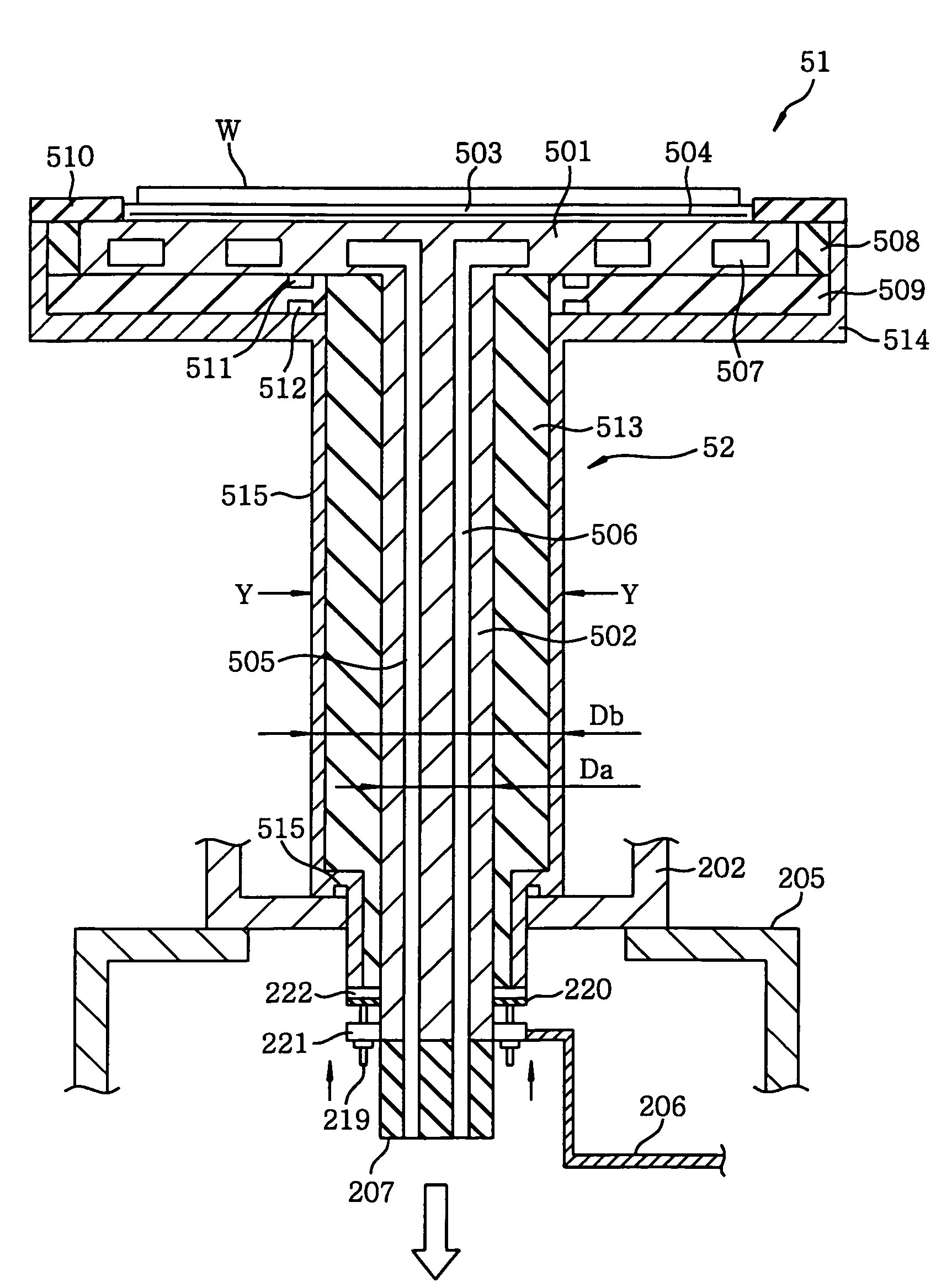
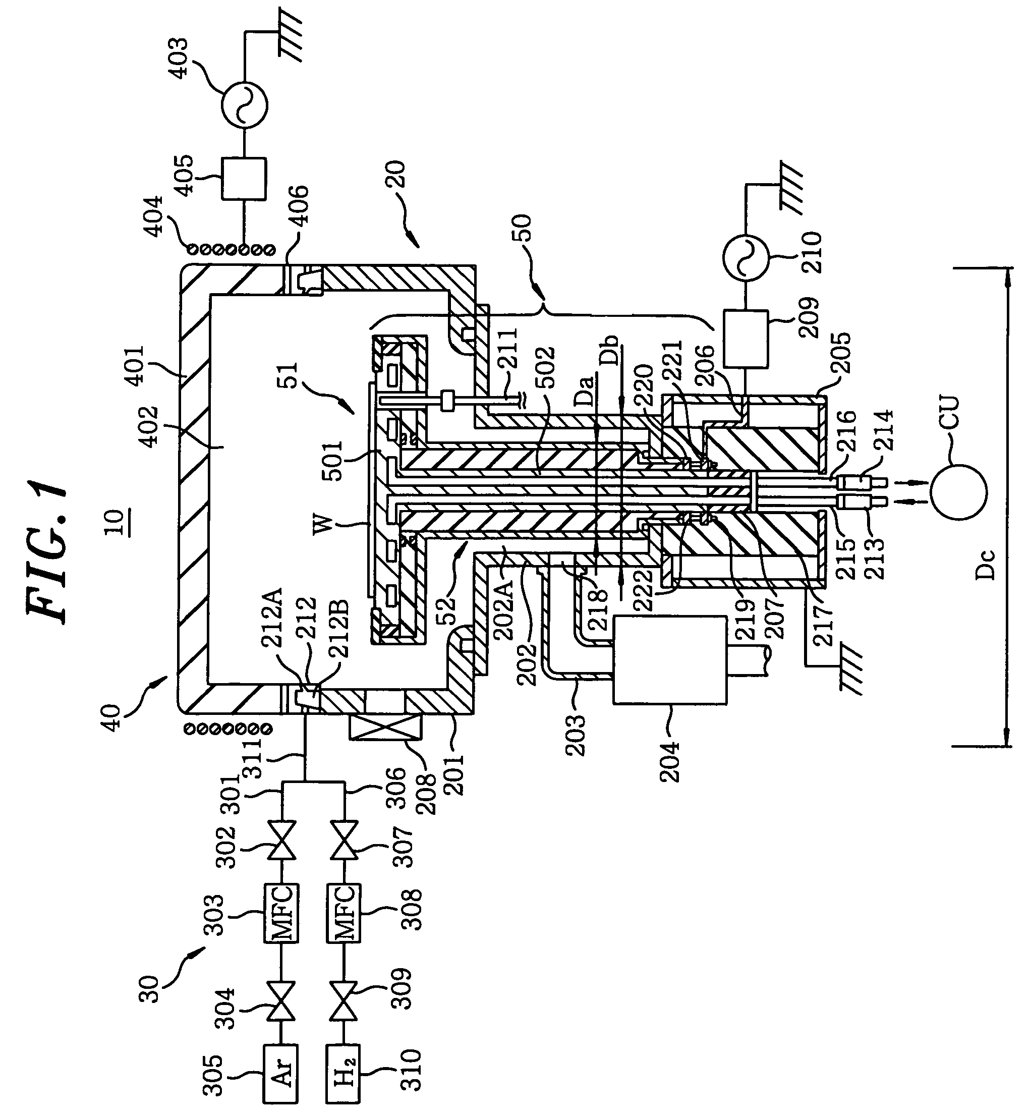
[0026]FIG. 1 is a configuration view showing a plasma processing device including a substrate supporting structure for semiconductor processing in accordance with a first embodiment of the present invention. A plasma processing device 10 is configured to perform a sputter etching or a reactive etching on a silicon oxide film, a metal oxide film or the like, which is formed on a semiconductor wafer as a substrate to be processed.

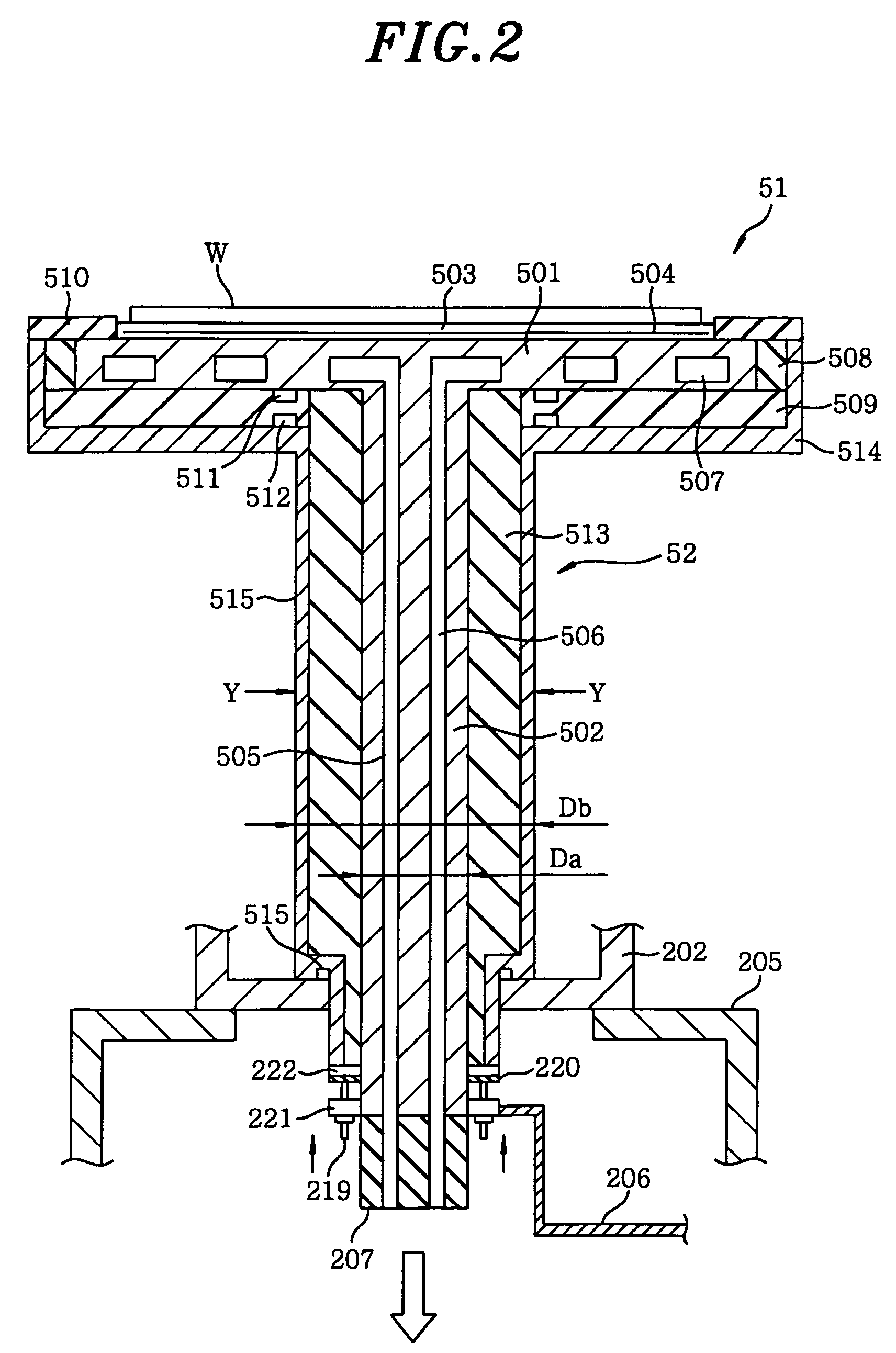
[0027]As shown in FIG. 1, the plasma processing device 10 includes a processing chamber 20 for receiving thereinto a substrate W to be processed. To the processing chamber 20, a gas supply unit 30 for supplying a processing gas thereinto is coupled. An excitation mechanism 40 for converting the processing gas into a plasma is disposed at an outer upper side of the processing chamber 20. A mounting table 51 of a substrate supporting structure 50 for supporting the substrate W to be processed is disposed at an inner lower side of the processing chamber 20.

[0028...

second embodiment

[0085]In the aforementioned plasma processing device 10, if the metal oxide formed on the surface of metal, e.g., copper, aluminum or the like, is etched, metal removed from the substrate W to be processed is scattered. Scattered metal is deposited onto the top surface of the insulating focus ring 510 around the substrate W to be processed, and thus, forming a metal film. If the metal film is grown, a discharge path may be formed between the substrate to be processed (semiconductor wafer) W and the conductive cover (pedestal conduction layer) 514, which is grounded, through the metal film. In this case, since charged particles on the metal film flow on the cover 514 as a current, there may be incurred a loss of the RF power supplied to the electrode part 501. For the same reason, the processing efficiency is lowered and the processing uniformity is deteriorated due to a decrease in the self-bias or abnormal discharge in the discharge path.

[0086]Further, an electromagnetic configurat...


PUM

PropertyMeasurementUnit
diameteraaaaaaaaaa
frequencyaaaaaaaaaa
dielectric constantaaaaaaaaaa

Abstract

A substrate supportingstructure (50) for semiconductor processing, comprising a mounting table (51) for placing a processed substrate (W) disposed in a processing chamber (20), wherein temperature control spaces (507) for storing the fluid used as a heat exchange medium are formed in the mounting table (51), a conductive transmission path (502) is disposed to lead a high frequency power to the mounting table (51), and flow channels (505, 506) feeding or discharging the heat exchange medium fluid to or from the temperature control spaces (507) are formed in the transmission path (502).

Description

[0001]This application is a Continuation-In-Part Application of PCT International Application No. PCT / JP03 / 016960 filed on Dec. 26, 2003, which designated the United States.FIELD OF THE INVENTION[0002]The present invention relates to a substrate supporting structure and a plasma processing device. The term “semiconductor processing” used herein implies various processes to manufacture a semiconductor device and / or a structure including wiring, electrodes, and the like connected to the semiconductor device on a substrate to be processed, by forming a semiconductor layer, an insulating layer, a conductor layer, and the like, after a predetermined pattern, on the substrate to be processed, e.g., a semiconductor wafer, an LCD (Liquid Crystal Display) or an FPD (Flat Panel Display).BACKGROUND OF THE INVENTION[0003]With the recent trend of highly integrated and high-performance semiconductor device, improvement in productivity of manufacturing the semiconductor is very essential to realiz...

Claims


Application Information

Patent Timeline
Patent Type & Authority Patents(United States)
IPC IPC(8): H01L21/00C23C14/00C23C16/00H01L21/3065H01J37/32H01L21/683
CPCH01J37/32431H01L21/6831H01L21/67109H01J2237/2001Y10T279/23H01L21/3065
Inventor IKEDA, TAROTANAKA, SUMIYAMAMOTO, KAORU
Owner TOKYO ELECTRON LTD
Why Eureka
Try Eureka