Semiconductor device having power supply system

a technology of power supply system and semiconductor, applied in the field of semiconductor devices, can solve the problems of restricted space for mounting capacitors, achieve the effects of reducing the number of components, reducing the size of the substrate, and dense implementation of semiconductor integrated circuits

Inactive Publication Date: 2010-12-14
LONGITUDE SEMICON S A R L
View PDF6 Cites 7 Cited by
  • Summary
  • Abstract
  • Description
  • Claims
  • Application Information

AI Technical Summary

Benefits of technology

[0016]In accordance with the foregoing embodiments, by dynamically controlling the impedance value of the variable impedance component, it is possible to realize a low impedance value of the power supply system over a wide band using a small number of chip components, without providing a number of different kinds of decoupling capacitors having different resonance frequencies. Reduction in the number of components results in minimization of the size of a substrate on which the semiconductor device is mounted. Therefore, it is possible to realize dense implementation of semiconductor integrated circuits and reduction in power supply noise thereof. Hence, it is possible to realize not only a small area but also low power supply noise in the semiconductor device and a printed circuit board which mount the semiconductor device. In addition, a low impedance value of the power supply system can be realized over a wide band even in small-sized semiconductor equipment such as a mobile phone in which electronic components are densely mounted on a printed circuit board and space for mounting capacitors is restricted.

Problems solved by technology

In addition, a low impedance value of the power supply system can be realized over a wide band even in small-sized semiconductor equipment such as a mobile phone in which electronic components are densely mounted on a printed circuit board and space for mounting capacitors is restricted.

Method used


Image

  • Semiconductor device having power supply system
  • Semiconductor device having power supply system
  • Semiconductor device having power supply system

Examples


first embodiment

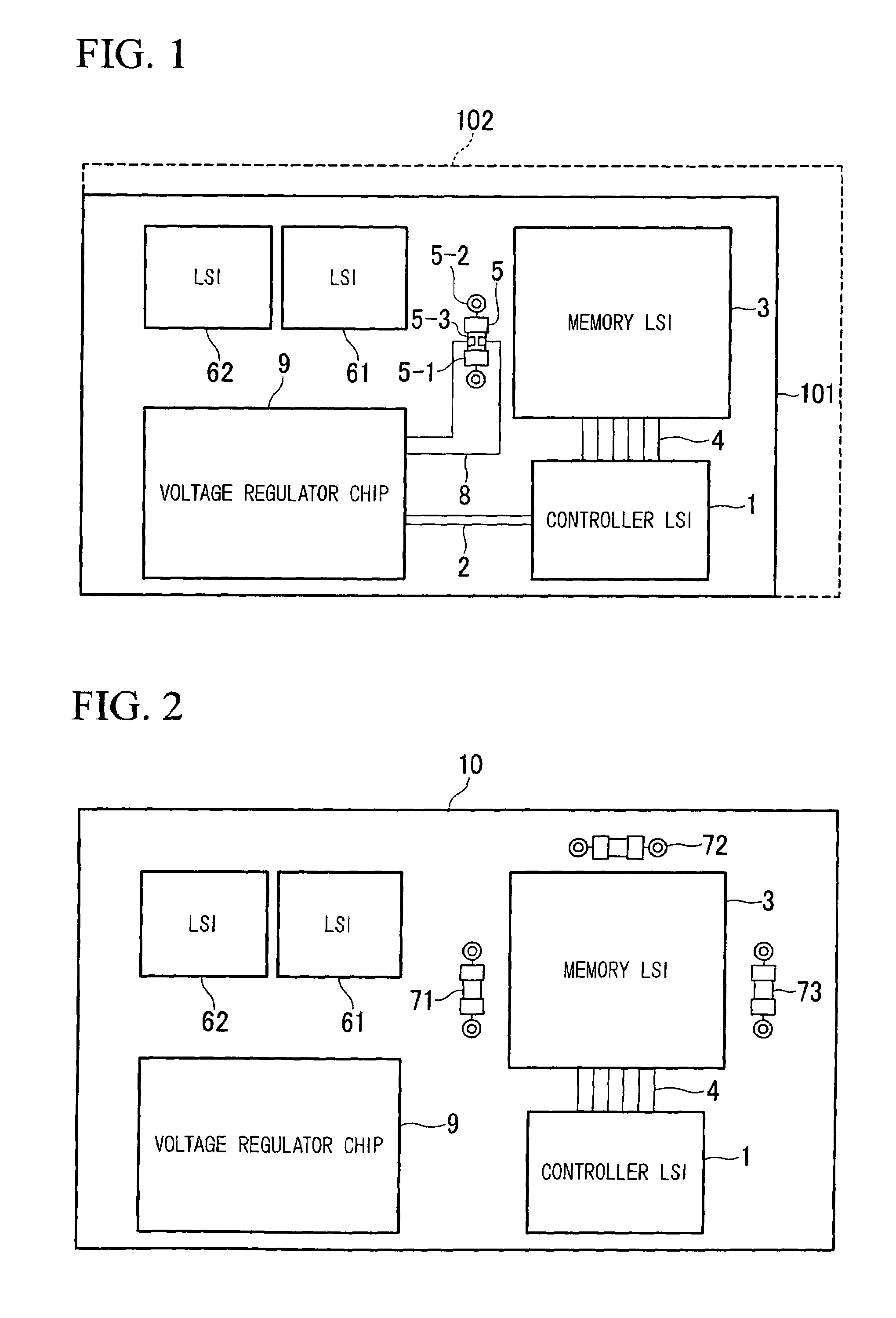
[0047]FIG. 1 is a diagram showing the structure of a semiconductor device in accordance with a first embodiment of the present invention.

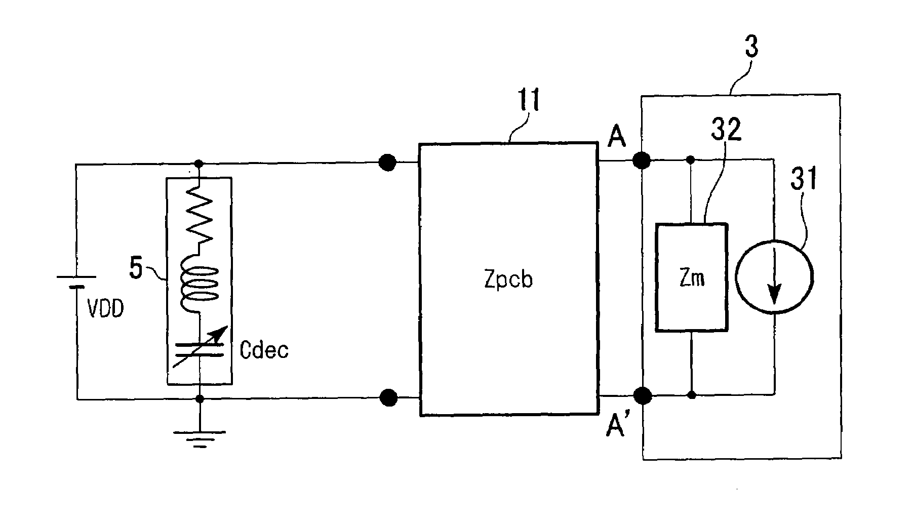
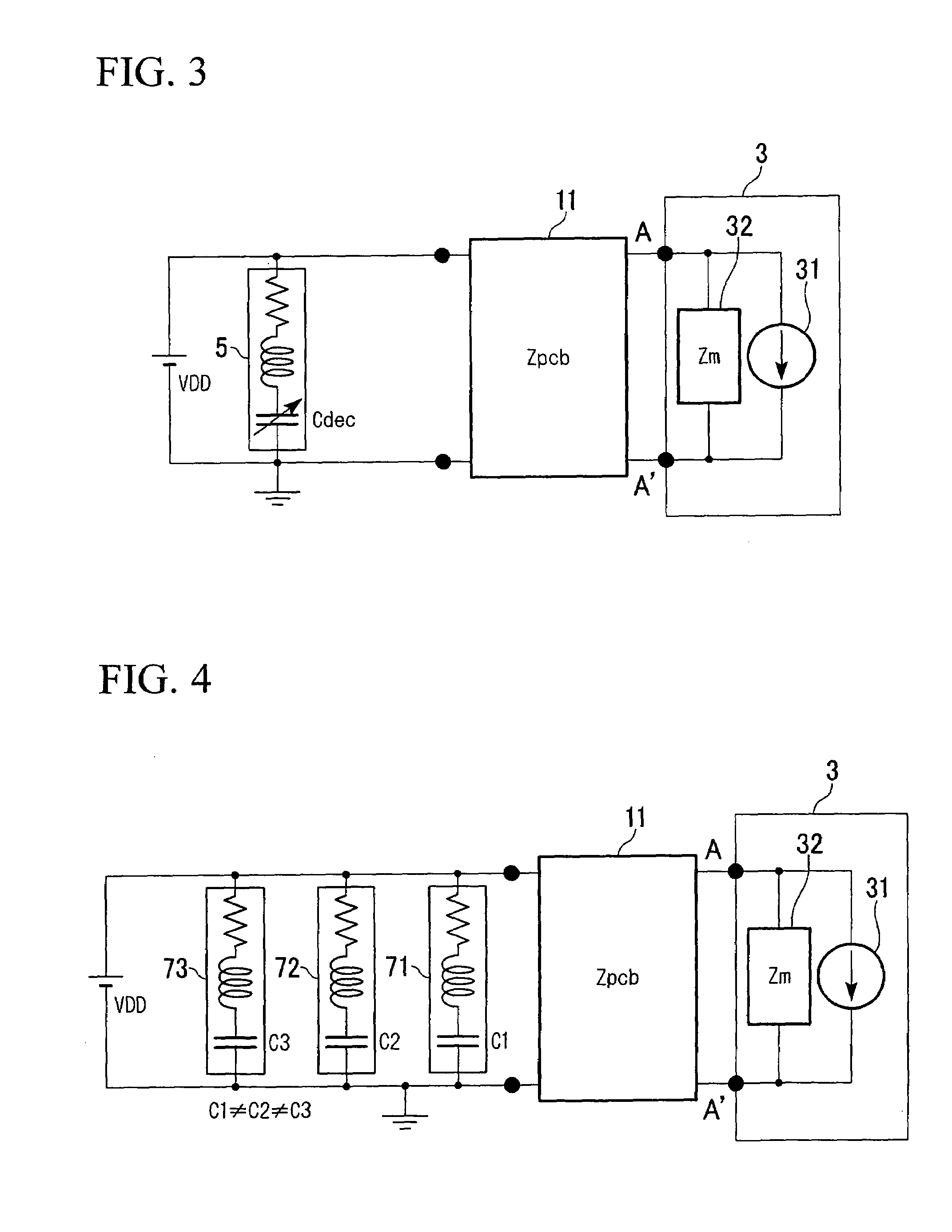
[0048]First, the structure of the semiconductor device in accordance with the first embodiment will be explained with reference to FIG. 1. On a printed circuit board 101, there are provided: a memory LSI 3 (a first semiconductor integrated circuit; e.g., a DRAM) in which noise is to be reduced; an on-board voltage regulator chip 9 (a second semiconductor integrated circuit); a controller LSI 1 (a third semiconductor integrated circuit) which controls the memory LSI 3; a decoupling capacitor 5 (a variable impedance component) which varies its own capacitance value in accordance with a bias voltage applied to a capacitance control terminal 5-3; LSIs 61 and 62; and so forth. A terminal 5-1 and a terminal 5-2 (a first terminal and a second terminal) of the decoupling capacitor 5 are respectively connected to a ground line and a power supply line which ...

second embodiment

[0062]In a second embodiment of the present invention, a capacitance-variable decoupling capacitor is provided in an LSI package, not on a printed circuit board. The second embodiment of the present invention will be explained with reference to FIG. 9. FIG. 9 is a diagram showing the structure of a semiconductor device in accordance with the second embodiment of the present invention.

[0063]FIG. 9 is characterized in that a decoupling capacitor 5 having a capacitance control terminal is provided in a package 18 which seals a memory LSI 3.

[0064]The fundamental concept and the structure of the present embodiment are the same as those in the first embodiment. By allowing the adjustment of the capacitance value of the decoupling capacitor 5, which is arranged at a position closer to the memory LSI 3 than that in the first embodiment, it is possible to dynamically adjust the impedance value even for noise having a higher frequency than that of the first embodiment. Therefore, the present ...

third embodiment

[0065]In a third embodiment of the present invention, a capacitance-variable decoupling capacitor is provided in a chip of a memory LSI. The third embodiment of the present invention will be explained with reference to FIG. 10. FIG. 10 is a diagram showing the structure of a semiconductor device in accordance with the third embodiment of the present invention.

[0066]The enlarged view in FIG. 10 shows an example of the structure of a MEMS-based capacitance-variable decoupling capacitor 5. As shown by the enlarged view in FIG. 10, the decoupling capacitor 5 includes upper electrodes 17 made of a piezoelectric material, which forms a pair with a lower metal electrode 19 formed on a Si substrate, thereby forming a parallel plate capacitor 15. The parallel plate capacitor 15 is a variable capacitor whose capacitance value varies in accordance with a voltage applied to the upper electrodes 17. The upper electrodes 17 bend in accordance with the externally applied voltage, thereby the dista...


PUM


Abstract

A semiconductor device is provided which includes: a first semiconductor integrated circuit; a ground line and a power supply line trough which electric power is supplied to the first semiconductor integrated circuit; and a variable impedance component which is connected between the ground line and the power supply line.

Description

BACKGROUND OF THE INVENTION[0001]1. Field of the Invention[0002]The present invention relates to semiconductor devices. More particularly, the present invention relates to a semiconductor device which is provided with a power supply system which supplies electric power to a semiconductor integrated circuit.[0003]Priority is claimed on Japanese Patent Application No. 2008-13559, filed Jan. 24, 2008, the content of which is incorporated herein by reference.[0004]2. Description of Related Art[0005]The inventors of the present invention investigated the following techniques in the art of semiconductor devices.[0006]In the art of semiconductor devices, it is becoming considerably difficult to design measures against power supply noise as with succeeding generations of LSIs (Large Scale Integrated circuits). Such difficulty is caused by an increase in current consumption of semiconductor elements which are required to operate at a high rate; an increase in power supply noise accompanied b...

Claims


Application Information

Patent Timeline
Patent Type & Authority Patents(United States)
IPC IPC(8): G05F1/10
CPCG06F1/26H01L23/50H01L2924/3011H01L2224/16225H01L2924/1461H01L2924/00
Inventor UEMATSU, YUTAKAOSAKA, HIDEKISAITO, TATUSYANISHIO, YOJI
Owner LONGITUDE SEMICON S A R L
Why Eureka
Try Eureka