

Thin film transistor array substrate and pixel structure with TFT having varying included angle of channel layer
a thin film transistor and array substrate technology, applied in non-linear optics, instruments, optics, etc., can solve the problems of threatening rc delay in the pixel structure, resistance-capacitance delay (rc delay) among the electronic devices of the lcd panel, color distortion or insufficient color saturation, etc., to achieve the effect of reducing the rc delay
- Summary
- Abstract
- Description
- Claims
- Application Information
AI Technical Summary
Benefits of technology
Problems solved by technology
Method used
Image

Examples
Embodiment Construction
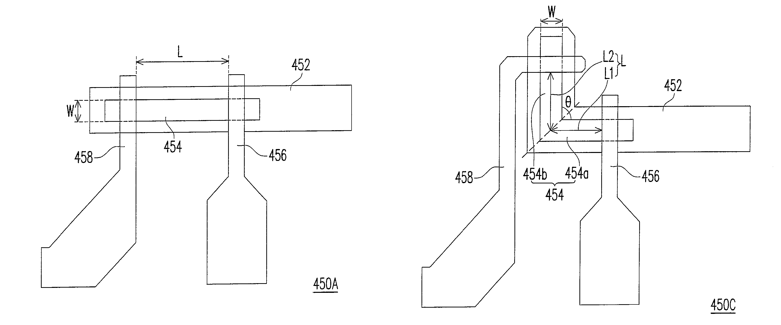
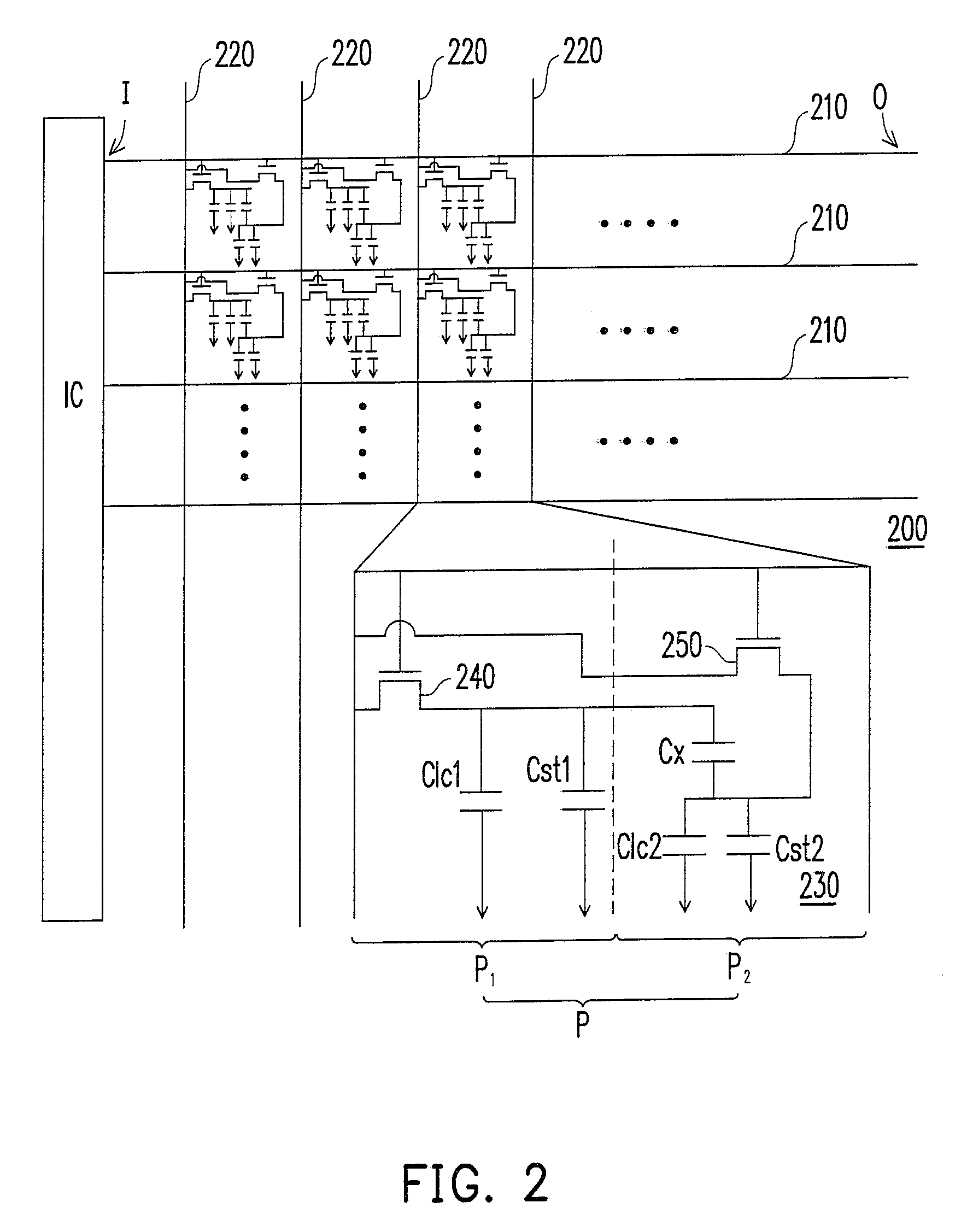
[0037]In general, each TFT on the same scan line in a TFT array substrate is required to achieve the same charging / discharging capacity so as to reduce an RC delay in an LCD panel. Accordingly, the present invention provides a design of a TFT array substrate. Through an alteration in a channel width and a channel length of the TFT, a larger W / L ratio of the TFT far away from a driving signal input terminal and a smaller W / L ratio of the TFT close to the driving signal input terminal can be accomplished. Here, the charging / discharging capacity of each TFT on the same scan line is almost identical.
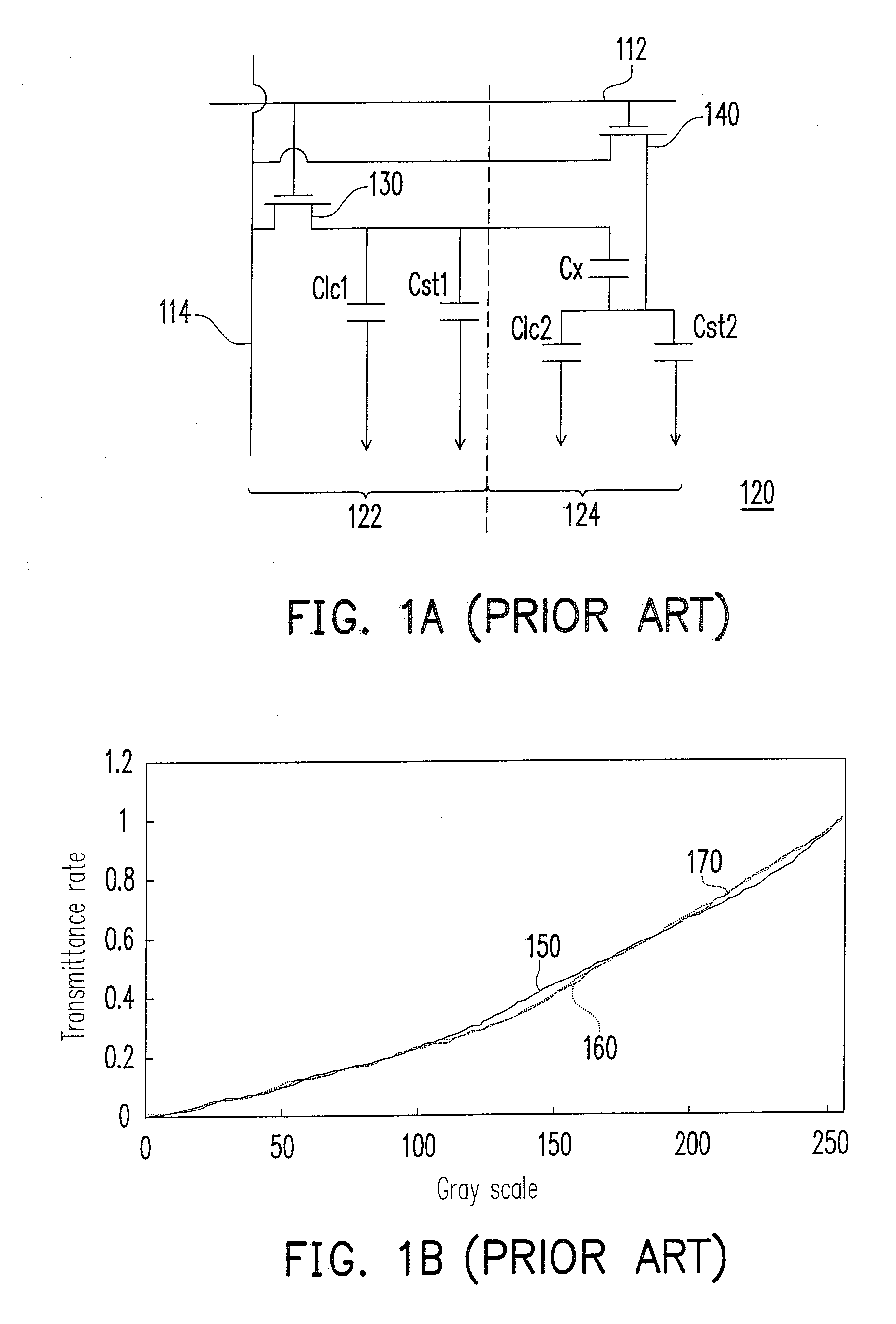
[0038]FIG. 2 is a schematic view of a TFT array substrate according to one embodiment of the present invention. Referring to FIG. 2, a TFT array substrate 200 includes a substrate (not shown), a plurality of scan lines 210, a plurality of data lines 220 and a plurality of pixel structures 230. The scan lines 210 are disposed on the substrate (not shown), and each scan line 210 includes a dri...
PUM
| Property | Measurement | Unit |
|---|---|---|
| included angle | aaaaa | aaaaa |
| included angles | aaaaa | aaaaa |
| included angles | aaaaa | aaaaa |
Abstract
Description
Claims
Application Information