

Electronic component
a technology of electronic components and components, applied in the direction of fixed capacitor details, thin/thick film capacitors, inductances, etc., can solve the problems of not always ensuring the required adhesion performance between the lower electrode layer and the dielectric layer, failure to achieve the required withstand voltage in the capacitor, and variable static capacitance characteristics of the capacitor, etc. achieve the effect of sufficient adhesion and facilitate the achievement of a high withstand voltag
Inactive Publication Date: 2010-12-21
FUJITSU LTD
View PDF14 Cites 3 Cited by
- Summary
- Abstract
- Description
- Claims
- Application Information
AI Technical Summary
Benefits of technology
The present invention provides an electronic component with a capacitor unit that has superior adhesion between the lower electrode layer and the dielectric layer, and achieves a higher withstand voltage. This is achieved by using an easily oxidizable metal layer as the adhesion metal layer, which is deposited on the surface of the lower electrode layer and joined to the dielectric layer via an oxide coating. The easily oxidizable metal layer has a high bonding performance with the dielectric layer, and the oxide coating facilitates the formation of a strong bond with the dielectric layer. The lower electrode layer can be joined to the dielectric layer with an adhesion layer containing the metal material of the adhesion metal layer, or with a main conductive layer containing a metal such as copper, silver, or aluminum. The electronic component can also include an interconnect layer on the substrate, which simplifies the selection of targets during a sputtering process.
Problems solved by technology
Insufficient adhesion between the layers provokes deterioration with time in adhesion status between those layers (for example, expansion of a gap between the layers with time), thus causing variation in static capacitance characteristic of the capacitor, which is undesirable.
Employing the Ti / Au / Ni / Au multilayer structure as the lower electrode layer, however, may not always assure the required adhesion performance between the lower electrode layer and the dielectric layer.
Also, employing the Ti / Au / Ni / Au multilayer structure as the lower electrode layer may lead to failure in attaining the withstand voltage of a required level in the capacitor.
Therefore, increasing the thickness of the dielectric layer is not a desirable solution, from the view point of suppressing an increase in dimensions of the capacitor, hence the IPD including the capacitor as a component.
Method used
View moreImage
Smart ImageViewing Examples

Examples
working example
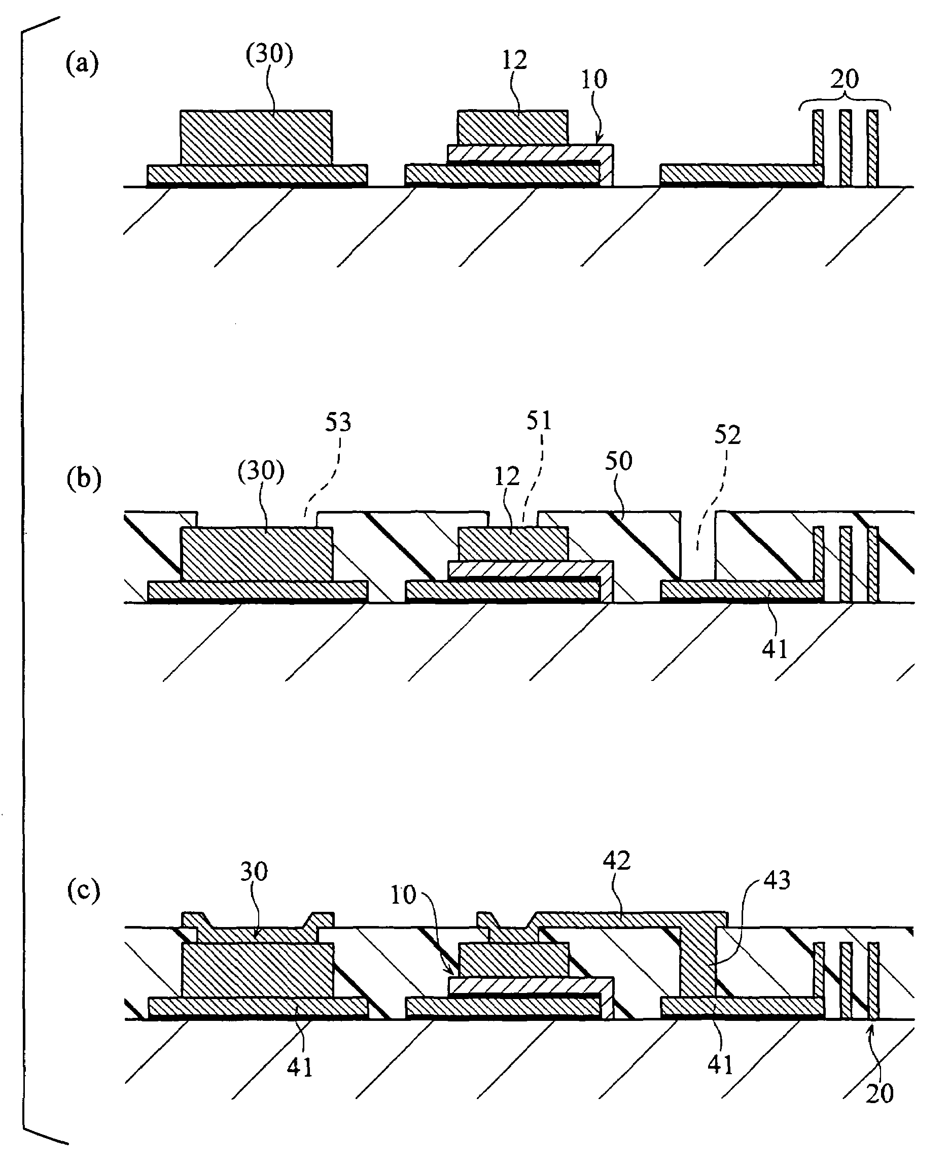
[0053]A plurality of capacitor elements was fabricated according to the present invention. When forming the respective capacitors, capacitor units having a laminate structure configured as FIG. 5 under the following conditions, were made on a glass substrate. The underlying adhesion layer 11a of the electrode layer 11 was a Ti layer of 50 nm in thickness. The main conductive layer 11b was a Au layer of 1000 nm in thickness. The adhesion metal layer 11c was a Ti layer of 50 nm in thickness, including an oxide coating on its surface. The electrode layer 12 was an electroplated Cu layer of 10 μm in thickness. The dielectric layer 13 was a SiO2 layer of 220 nm in thickness.
Login to View More PUM
| Property | Measurement | Unit |
|---|---|---|
| voltage | aaaaa | aaaaa |
| thickness | aaaaa | aaaaa |
| thickness | aaaaa | aaaaa |
Abstract
An electronic component includes a substrate, and a capacitor unit on the substrate. The capacitor unit has a laminate structure including a first electrode layer provided on the substrate, a second electrode layer opposed to the first electrode layer, and a dielectric layer disposed between the first and the second electrode layers. The first electrode layer has a multilayer structure including an adhesion metal layer joined to the dielectric layer. The adhesion metal layer is provided with an oxide coating on a side of the dielectric layer.
Description
BACKGROUND OF THE INVENTION[0001]1. Field of the Invention[0002]The present invention relates to an electronic component that includes a capacitor provided on a substrate, for example formed by semiconductor processing technology.[0003]2. Description of the Related Art[0004]In a radio frequency (hereinafter, RF) system such as a mobile phone or a wireless LAN, signals have to be subjected to phase-matching for satisfactory transmission among functional devices constituting the system. Accordingly, the input / output terminal of each device is generally provided with a passive component such as an inductor or a capacitor, and that acts as a phase shifter for controlling the phase of the signals.[0005]In the RF system in general, a SAW filter is employed for use as a narrow-band frequency filter. The SAW filter, which includes a piezoelectric element, produces a difference in potential between piezoelectric element electrodes because of a piezoelectric effect, when a physical impact or ...
Claims
Login to View More Application Information
Patent Timeline
 Patent Type & AuthorityPatents(United States)
IPC IPC(8): H01L23/48H01L23/52H01L29/40
CPCH01G4/008H01G4/232H01L24/18H01L28/10H01L28/75H01G4/33H01L27/04
InventorMATSUMOTO, TSUYOSHIMIZUNO, YOSHIHIROMI, XIAOYUOKUDA, HISAOUEDA, SATOSHI
OwnerFUJITSU LTD