Wireless chip

a technology of wireless chips and wires, applied in the structure of radiating elements, instruments, resonant antennas, etc., can solve the problems of disposal methods and recycling, risk of unexpected accidents, skin or drinking injury, etc., and achieves favorable communication properties, small size, and high safety.

Inactive Publication Date: 2011-01-04
SEMICON ENERGY LAB CO LTD
View PDF34 Cites 15 Cited by
  • Summary
  • Abstract
  • Description
  • Claims
  • Application Information

AI Technical Summary

Benefits of technology

[0005]The invention provides a wireless chip which is small in size, favorable in communication property, and inexpensive and which can ensure the safety of the ultimate consumer, and an application thereof. Furthermore, the invention provides a wireless chip which can be recycled after being used for managing the manufacture, circulation, and retail.
[0016]The invention can provide a wireless chip which is small in size, favorable in communication property, and inexpensive by forming an antenna using a dielectric with a high dielectric constant or a magnetic body.
[0017]Further, the invention can provide a wireless chip with high safety which does not cause an injury or the like when touched, by forming an outer shape of a dielectric layer which forms the outer shape of the wireless chip so as to have only a flat surface and a curved surface.
[0018]The invention can provide a wireless chip with high safety which does not harm a human body even when the wireless chip is drunk by mistake, by coating the outermost surface with a resin or DLC (Diamond-Like Carbon) so as to have a shape with a curved surface. Moreover, the physical strength of the wireless chip is enhanced by coating the outermost surface thereof, which leads to a recyclable wireless chip which can be used repeatedly.
[0019]Furthermore, in the case of attaching a wireless tag to a product, a wireless tag may be wrapped with paper, plastic, cloth, or the like or incorporated in a bag, a box, a free gift, or the like. Accordingly, the wireless chip can be safely used by forming the outermost surface thereof with a material and a shape with high safety and a size and a shape that the consumers can easily recognize the wireless tag.

Problems solved by technology

Therefore, for example, there is a risk of an unexpected accident such as injuring skin or drinking by mistake.
Moreover, there is a problem in the disposal method and recycling since a large number of wireless chips are used when used for retail.

Method used


Image

  • Wireless chip
  • Wireless chip
  • Wireless chip

Examples


embodiment mode 1

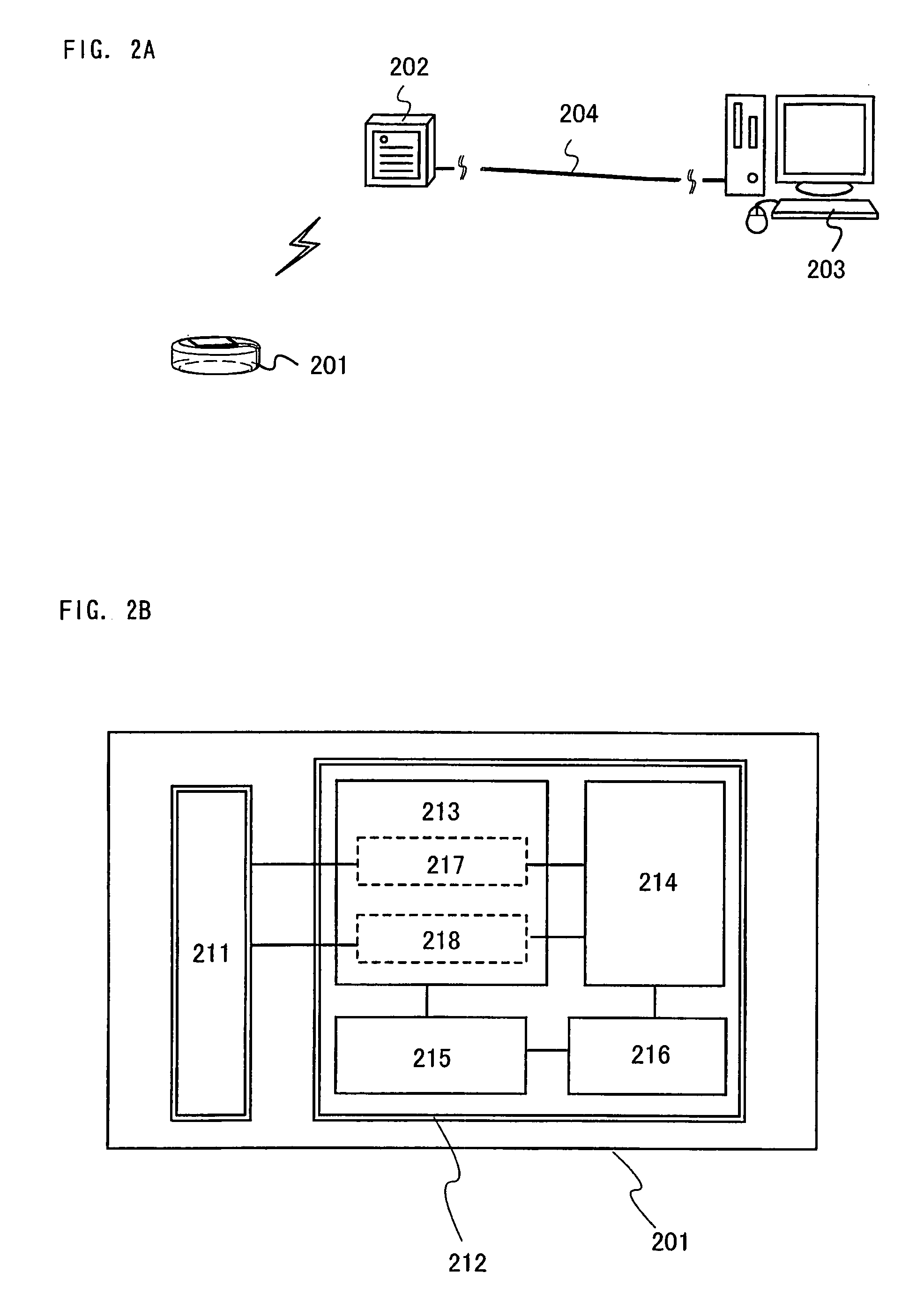
[0044]As shown in FIG. 2A, the wireless chip 201 of the invention wirelessly communicates with the reader / writer 202. The wireless chip 201 generally operates by receiving power supply from the reader / writer 202 through electromagnetic waves for communication. Receiving the data transmitted from the reader / writer 202, the wireless chip 201 determines right or wrong thereof and sends back the stored data to the reader / write 202 when the data is right. Furthermore, the wireless chip 201 stores and erases the data based on the instruction received from the reader / writer 202.

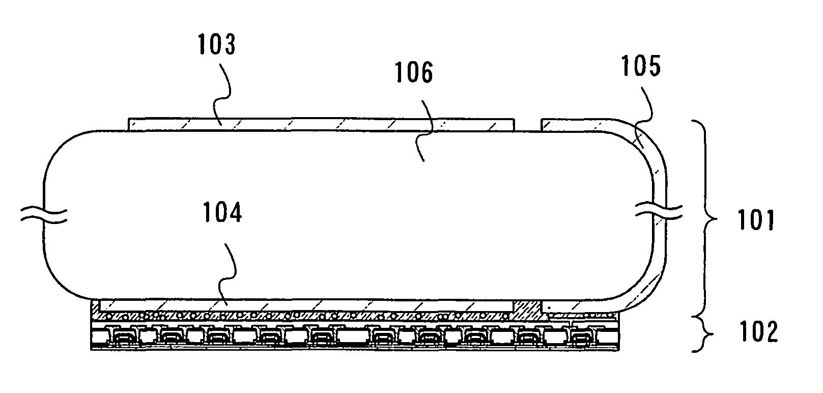
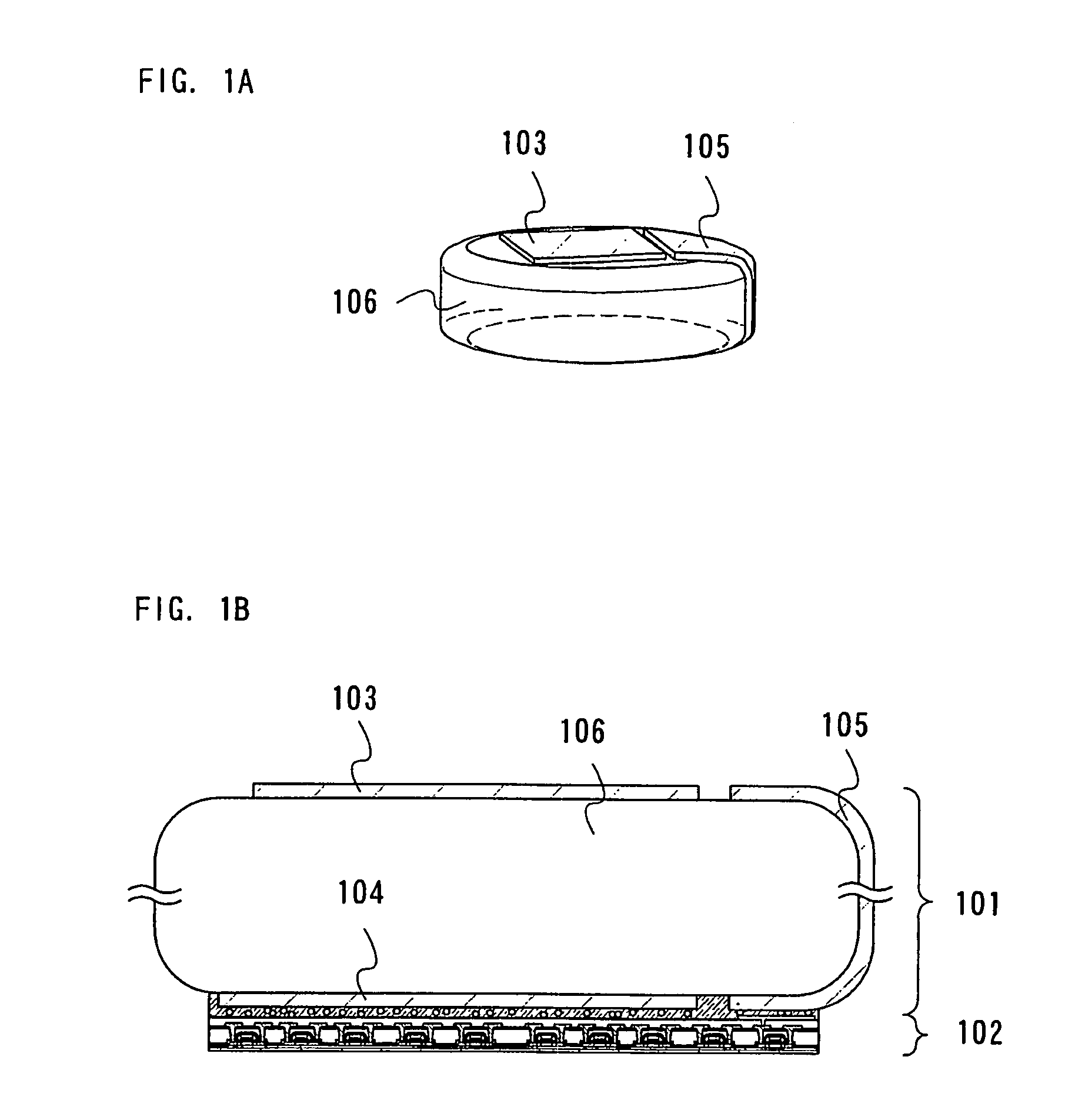
[0045]FIGS. 1A and 1B show a wireless chip of the invention with the aforementioned configuration. FIG. 1A is a perspective view showing an example of an appearance of the wireless chip and FIG. 1B is a sectional view of the wireless chip.

[0046]As shown in FIG. 1A as an example, the wireless chip of the invention has a cylindrical shape and a curved surface in an outer edge portion. In specific, corners at which a t...

embodiment mode 2

[0103]In this embodiment mode, description is made on a different manufacturing method of the wireless chip of the invention with the function described in Embodiment Mode 1.

[0104]As shown in FIG. 7A, a wireless chip of this embodiment mode includes a layer 701 including a semiconductor element and an antenna 703. The layer 701 including a semiconductor element has a semiconductor element such as a field effect transistor over a semiconductor substrate formed of silicon or the like. Moreover, the antenna may be similar to the antenna described in Embodiment Mode 1.

[0105]In the wireless chip of this embodiment mode, the antenna 703 and the layer 701 including a semiconductor element are connected through conductive layers 702a and 702b. In specific, a connecting terminal 704a formed over the surface of the layer 701 including a semiconductor element is connected to a power feeding layer 713 of the antenna through the conductive layer 702a. Then, a connecting terminal 704b formed over...

embodiment mode 3

[0135]This embodiment mode describes steps of forming the semiconductor element in the layer including a semiconductor element described in Embodiment Modes 1 and 2 by using different materials. In this embodiment mode, a layer including a semiconductor element is formed by forming a semiconductor element having an organic semiconductor layer over an insulating substrate as an example.

[0136]For example, a flexible substrate has lower thermal resistance as compared to a non-flexible substrate such as a glass substrate. Therefore, in the case of forming a semiconductor element over a flexible substrate, it is preferable to use an organic semiconductor. The layer including a semiconductor element formed of an organic semiconductor is formed by forming a semiconductor element over a flexible substrate and an insulating layer to cover the semiconductor element. A connecting terminal to be connected to a wire of the semiconductor element is formed over the surface of the layer including t...


PUM


Abstract

The invention provides a wireless chip which can secure the safety of consumers while being small in size, favorable in communication property, and inexpensive, and the invention also provides an application thereof. Further, the invention provides a wireless chip which can be recycled after being used for managing the manufacture, circulation, and retail. A wireless chip includes a layer including a semiconductor element, and an antenna. The antenna includes a first conductive layer, a second conductive layer, and a dielectric layer sandwiched between the first conductive layer and the second conductive layer, and has a spherical shape, an ovoid shape, an oval spherical shape like a go stone, an oval spherical shape like a rugby ball, or a disc shape, or has a cylindrical shape or a polygonal prism shape in which an outer edge portion thereof has a curved surface.

Description

TECHNICAL FIELD[0001]The invention relates to a wireless chip which communicates wirelessly through electromagnetic waves.BACKGROUND ART[0002]In recent years, an automatic recognition technique which is constituted by a wireless chip which stores data in its electronic circuit, a reader / writer which reads and writes data stored in the wireless chip, and a host system which processes the read data, controls the reader / writer, or the like has been developed and introduced (see FIGS. 2A and 2B). A wireless chip 201 is called by various names such as an RFID tag, an IC tag, and a wireless tag, however, as a specific name does not exist, it is called a wireless chip in this specification. The wireless chip 201 basically has no battery and performs a dielectric operation by electromagnetic waves emitted from the reader / writer 202 to wirelessly communicate with the reader / writer 202. Moreover, a computer 203 is generally used as a host system which communicates with the reader / writer 202 t...

Claims


Application Information

Patent Timeline
Patent Type & Authority Patents(United States)
IPC IPC(8): H01Q1/38
CPCG06K19/04G06K19/07749H01Q1/38H01L27/1266H01L27/1214G06K19/077H01L23/12G06K19/07775
Inventor YAMAZAKI, SHUNPEIIZUMI, KONAMI
Owner SEMICON ENERGY LAB CO LTD
Why Eureka
Try Eureka