Optoelectronic component and package for an optoelectronic component

a technology of optoelectronic components and components, applied in the direction of basic electric elements, electrical apparatus, semiconductor devices, etc., can solve the problems of segregation effects, adversely affecting the yield of mass production, and difficult to introduce the intended amount of luminescent material at the intended location

Inactive Publication Date: 2011-02-22
OSRAM OPTO SEMICONDUCTORS GMBH
View PDF35 Cites 16 Cited by
  • Summary
  • Abstract
  • Description
  • Claims
  • Application Information

AI Technical Summary

Benefits of technology

[0006]It is, in particular, an object of the present invention to provide an optoelectronic component with which a re...

Problems solved by technology

In particular in the case of so-called conversion LEDs, in which at least part of the radiation emitted by the semiconductor chip (hereafter primary radiation) is converted by a luminescent material in the casting compound into radiation with an at least partly changed wavelength in comparison with the primary radiation, it is technically often difficult to introduce the intended amount of luminescent ...

Method used


Image

  • Optoelectronic component and package for an optoelectronic component
  • Optoelectronic component and package for an optoelectronic component
  • Optoelectronic component and package for an optoelectronic component

Examples


Embodiment Construction

[0032]In the exemplary embodiments and associated figures, component parts that are the same or act in the same way are respectively provided with the same reference numerals. The elements represented in the figures, in particular the layer thicknesses, are not to be regarded as true to scale. Rather, they may in some cases be exaggerated for better understanding.

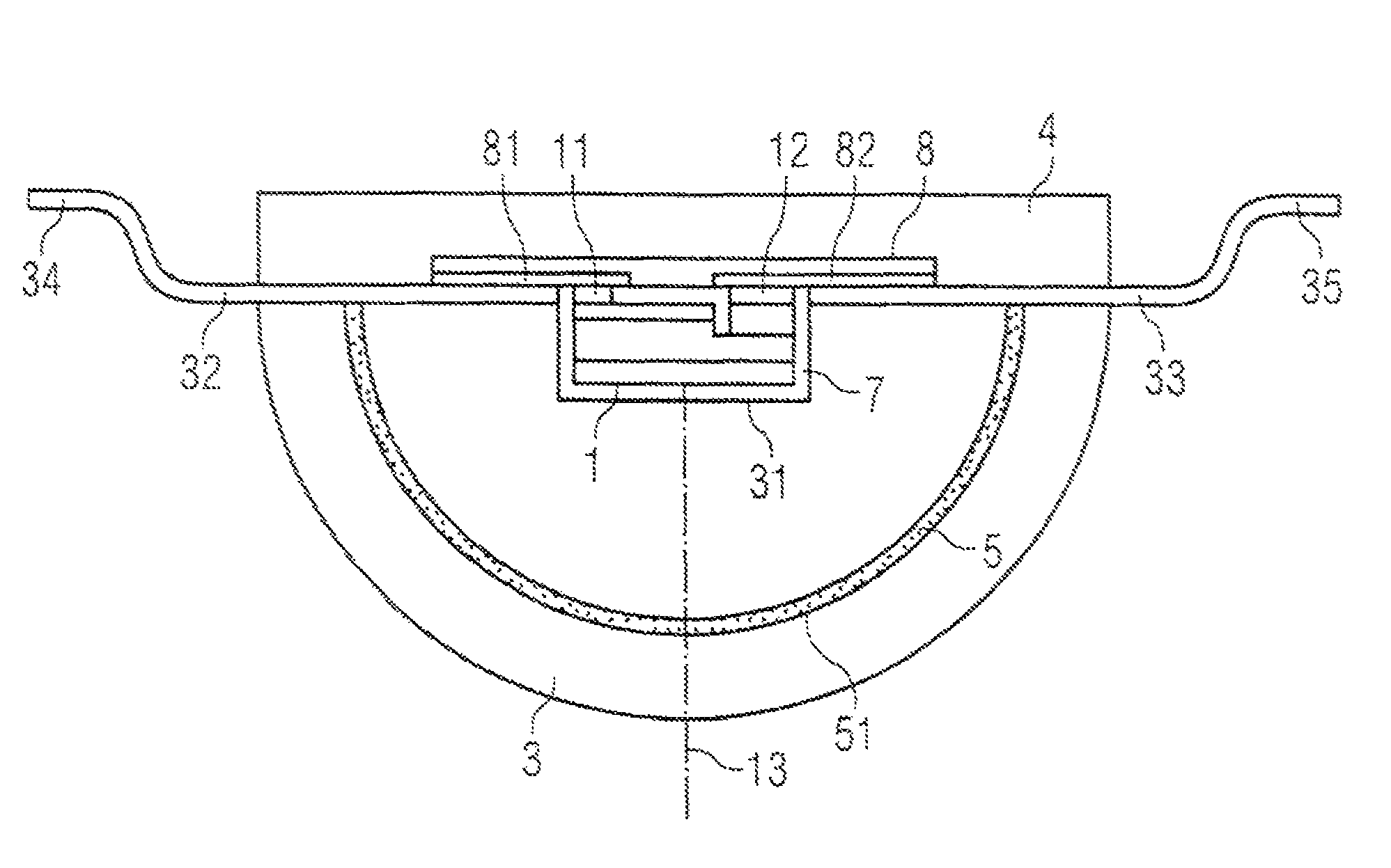
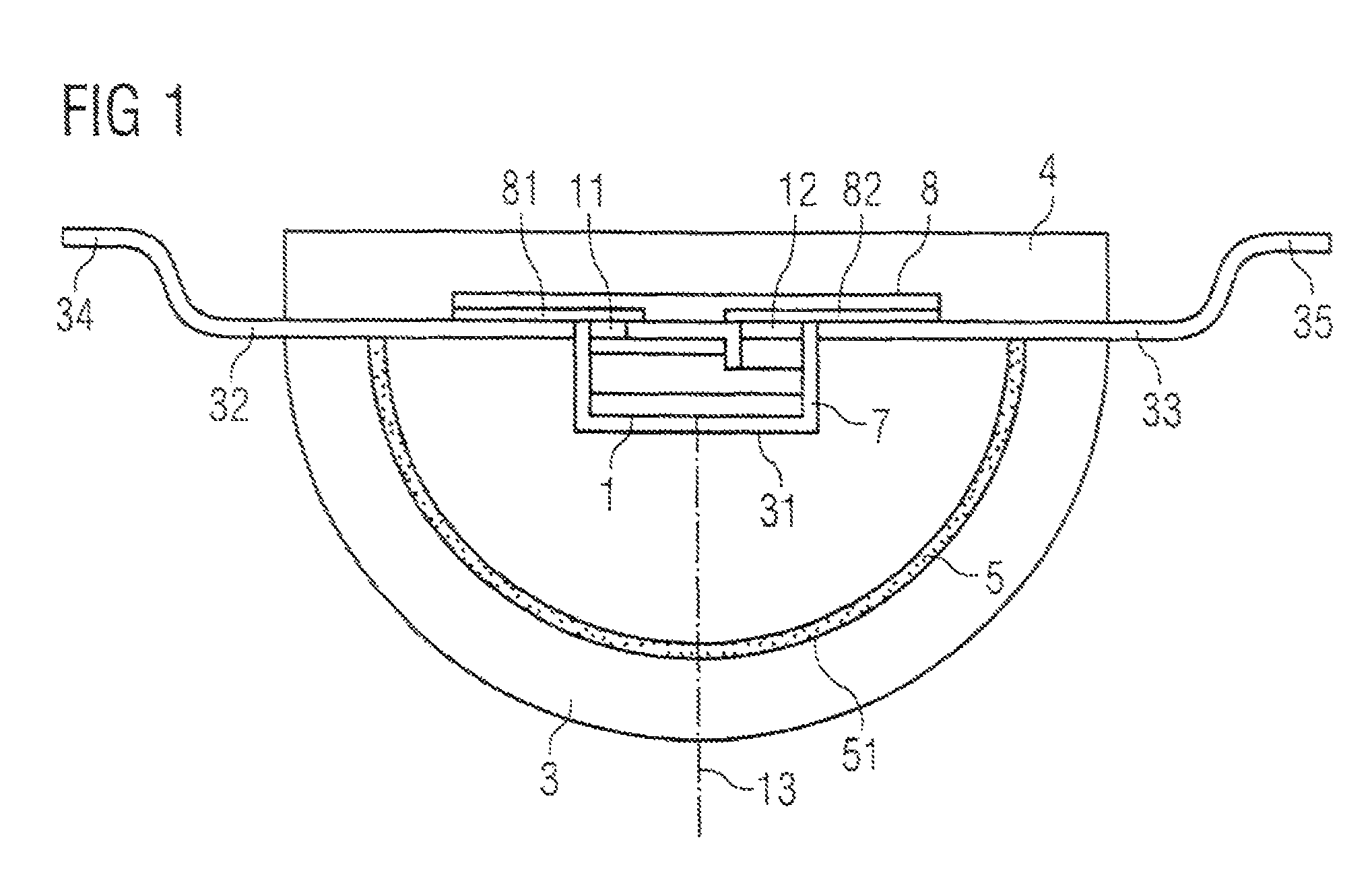
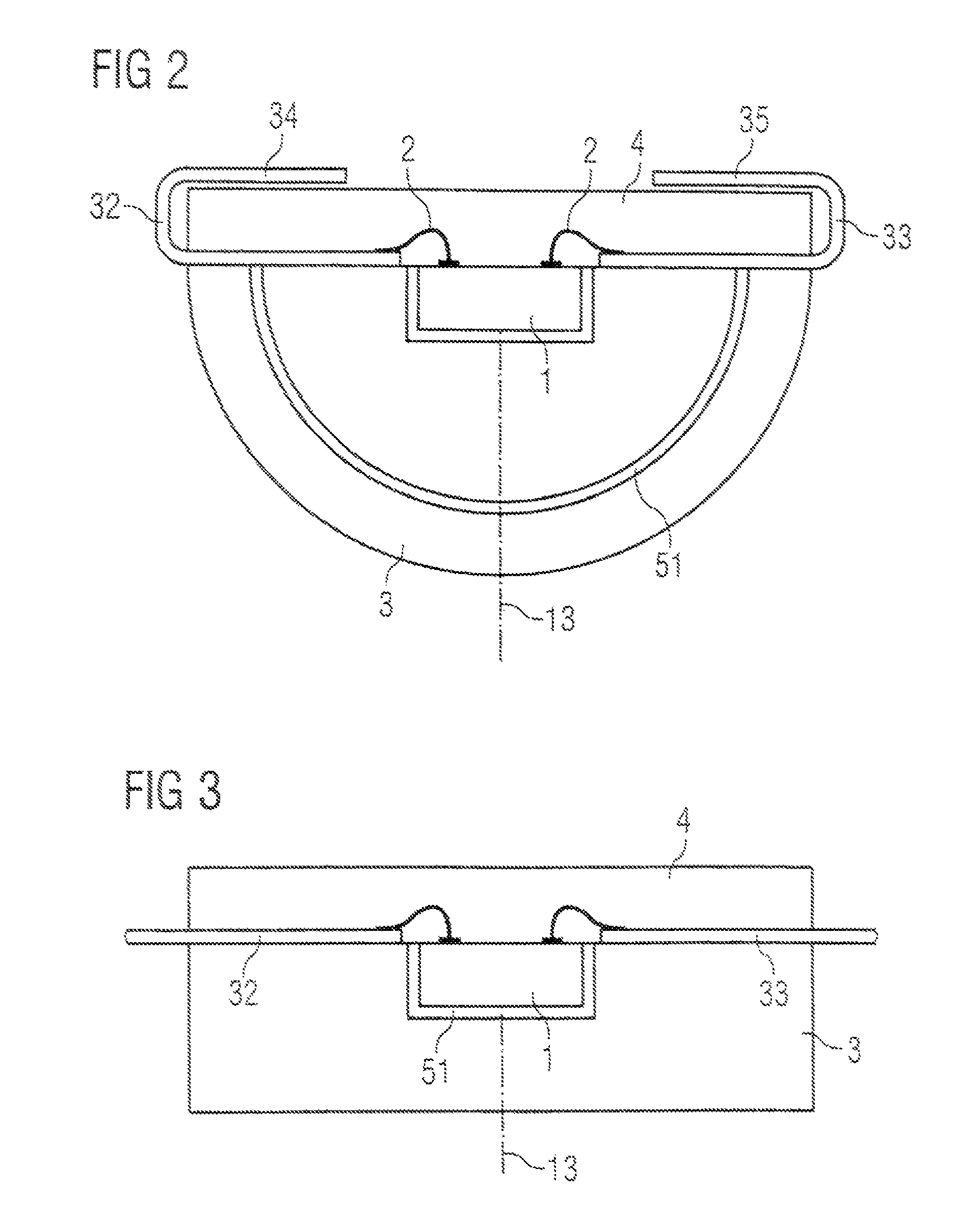
[0033]In the case of the exemplary embodiment according to FIG. 1, a basic package body 3 shaped in a hemispherical manner has a recess 31 on the side of the basic package body 3 facing away from the hemispherically curved surface. Embedded in the basic package body 3 is a luminescence conversion, material 5 in the form of a converter layer 51, which runs parallel to the hemispherically curved surface. That is to say that the converter layer 51 has, for example, the same or substantially the same curvature as the hemispherically curved surface. On account of its hemispherical form, the package body 3 acts as a beam-focusing...


PUM


Abstract

Optoelectronic components with a semiconductor chip, which is suitable for emitting primary electromagnetic radiation, a basic package body, which has a recess for receiving the semiconductor chip and electrical leads for the external electrical connection of the semiconductor chip and a chip encapsulating eclement, which encloses the semiconductor chip in the recess. The basic package body is at least partly optically transmissive at least for part of the primary radiation and an optical axis of the semiconductor chip runs through the basic package body The basic package body comprises a luminescence conversion material, which is suitable for converting at least part of the primary radiation into secondary radiation with wavelengths that are at least partly changed in comparison with the primary radiation.

Description

CROSS-REFERENCE TO RELATED APPLICATIONS[0001]This application is the National Stage of International Application No, PCT / DE2005 / 001735, filed on Sep. 28, 2005, which claims the priority to German Patent Application Serial No. 10 2004047640.3, filed on Sep. 30, 2004. The contents of both applications are hereby incorporated by reference in their entireties.FIELD OF THE INVENTION[0002]The invention relates to an optoelectronic component and to a package for an optoelectronic component.BACKGROUND OF THE INVENTION[0003]Surface-mountable (SMD) light-emitting diode components (LEDs) in leadframe technology are often mounted in a transfer-moulded or injection-moulded plastic package body prefabricated on the leadframe, are connected there to electrical leads and, for protection against harmful external influences, are encapsulated with a transparent casting compound, through, which light is coupled out during the operation of the LEDs.[0004]In particular in the case of so-called conversion...

Claims


Application Information

Patent Timeline
IPC IPC(8): H01L31/00H01L33/50
CPCH01L33/507H01L2224/48091H01L2224/48247H01L2224/73265H01L2924/00014
Inventor HARLE, VOLKER
Owner OSRAM OPTO SEMICONDUCTORS GMBH
Why Eureka
Try Eureka