Detachable substrate with controlled mechanical strength and method of producing same

a technology of mechanical strength and detachable substrates, which is applied in the direction of microstructural technology, electric devices, solid-state devices, etc., can solve the problems of excessive cost of original substrates that are beneficial for the production of components, inability to transfer to another support, and inability to meet the requirements of high-resistance substrates

Inactive Publication Date: 2011-03-08
COMMISSARIAT A LENERGIE ATOMIQUE ET AUX ENERGIES ALTERNATIVES
View PDF210 Cites 47 Cited by
  • Summary
  • Abstract
  • Description
  • Claims
  • Application Information

AI Technical Summary

Benefits of technology

[0031]The step of producing the interface is followed by a step of lifting off the two wafers; a step of producing all or part of micro-electronic, opto-electronic, mechanical, pyro-electric, superconductor or magnetic components can be executed after detachment. Between the step of producing the interface and the lifting off step, another bonding step can advantageously be executed to create a second interface. This bonding step advantageously includes molecular adhesion bonding or adhesive bonding (for example using an adhesive hardened by UV radiation, a resin, a polymer adhesive). In this case, a lift-off step at the level of the second interface can advantageously be carried out by acid etching and / or application of mechanical stresses and / or thermal and / or photonic stresses. The wafer that has not been processed or transferred can advantageously be used again after lift-off.

Problems solved by technology

However, a highly resistive substrate is not necessarily available at the same cost and with the same quality as the standard substrates usually employed.
There may also be cited situations in which the original substrate that is beneficial for the production of the components is excessively costly.
In some cases the transfer to another support is not indispensable, especially if the final thickness aimed at during thinning is sufficient to produce self-supporting structures.
A problem then arises in choosing the means employed to assemble the layer and the substrate.
More generally, the problem that arises is that of assembling a wafer with another wafer, which wafers can be substrates, thin layers, or sufficiently thick to be self-supporting, composite or otherwise, composed of at least one or more semiconductor materials, partly, completely processed or unprocessed, the assembly having to be separated thereafter at the assembly interface.
The first solution consists in eliminating the support wafer by abrasion, but in this case the wafer is consumed (destroyed during the process).
However, these techniques based on lifting off depend on the fact that it is difficult to obtain lift-off on a lateral scale exceeding 1 mm.
If the structure is bonded sufficiently strongly to another substrate and a high stress is applied to the structure, uncontrolled fracture, preferentially achieved in the oxide, can lead to a cutting effect on the scale of the entire substrate.
Unfortunately, the fracture is difficult to control and necessitates high mechanical stresses to bring it about, which is not free of the risk of breaking of the substrate or damaging the components.
Sealing with energies of this magnitude is incompatible with detachment.

Method used


Image

  • Detachable substrate with controlled mechanical strength and method of producing same
  • Detachable substrate with controlled mechanical strength and method of producing same
  • Detachable substrate with controlled mechanical strength and method of producing same

Examples


Embodiment Construction

roduction of components,

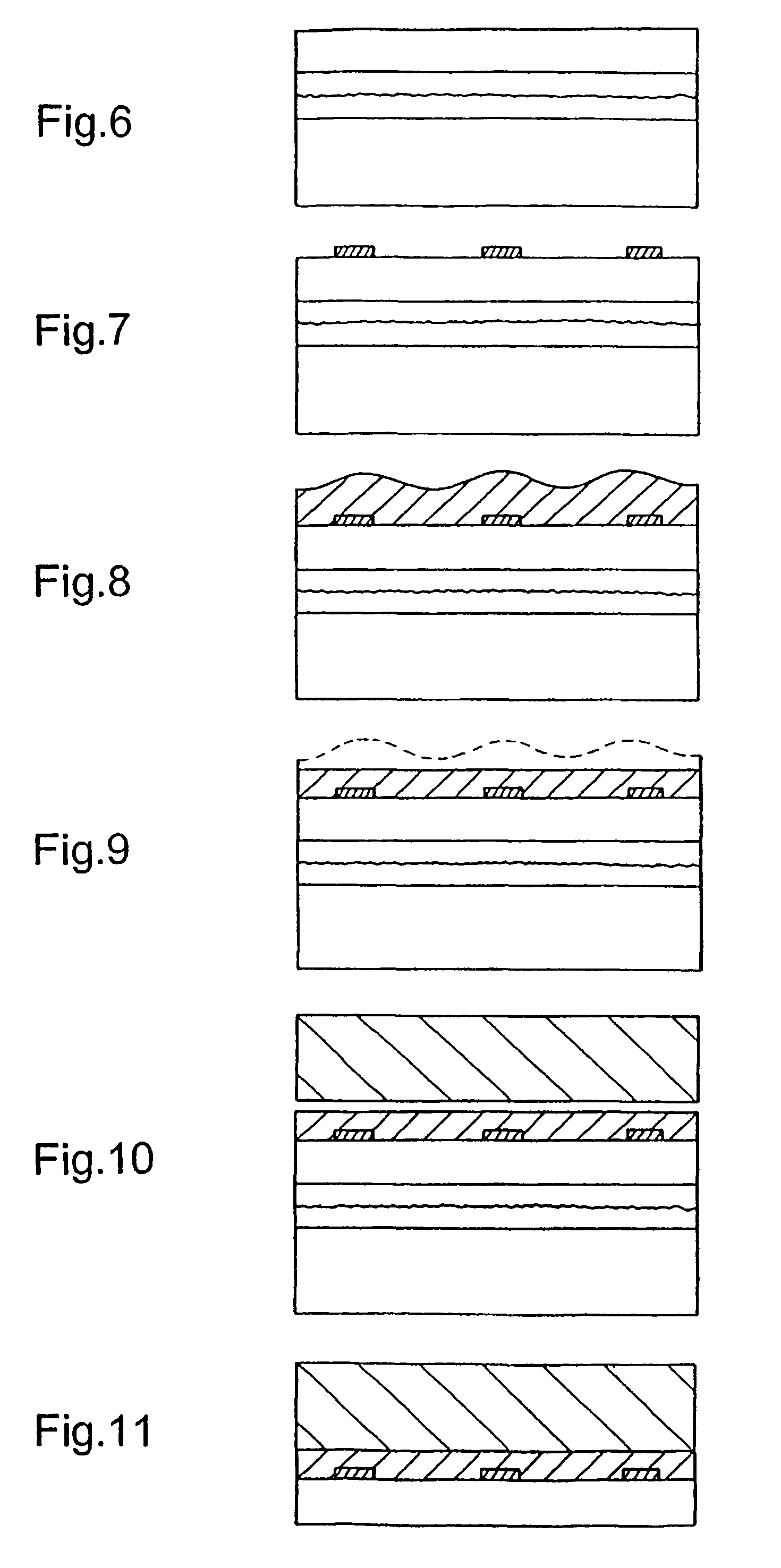
[0059]FIG. 14 is a view thereof during detachment by hydrofluoric acid etching and / or application of mechanical forces without transfer to a target substrate,

[0060]FIG. 15 is a view thereof after detachment into a final substrate and a substrate that can be recycled,

[0061]FIG. 16 is a variant of FIG. 13, after cutting trenches or notches between the components,

[0062]FIG. 17 is a view thereof showing a component being lifted off, for example after hydrofluoric acid etching,

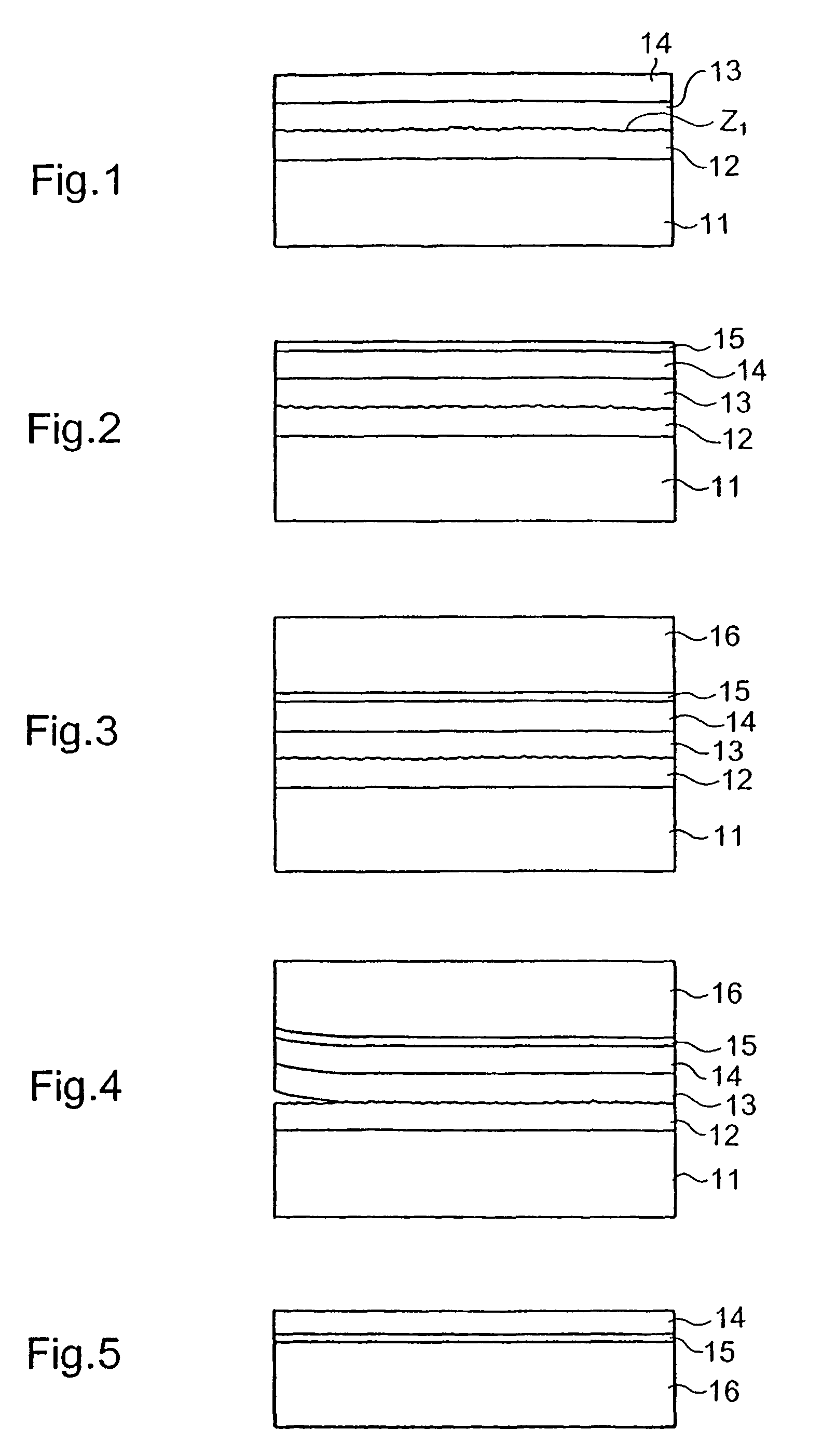
[0063]FIG. 18 is a view analogous to FIG. 1,

[0064]FIG. 19 is a diagrammatic view in section of the FIG. 3 assembly after adhesive bonding of a transparent substrate,

[0065]FIG. 20 is a view of the upper portion of this assembly after lifting off and polishing,

[0066]FIG. 21 is a view of the upper portion of this assembly after lifting off and polishing,

[0067]FIG. 22 is an overall view analogous to that of FIG. 1, showing regions that are eliminated by chemical and mechanical cutting,

[0068]FIG....


PUM

PropertyMeasurementUnit
sizeaaaaaaaaaa
sizeaaaaaaaaaa
resistivityaaaaaaaaaa

Abstract

The invention relates to a method for production of a detachable substrate, comprising a method step for the production of an interface by means of fixing, using molecular adhesion, one face of a layer on one face of a substrate, in which, before fixing, a treatment stage for at least one of said faces is provided, rendering the mechanical hold at the interface at such a controlled level to be compatible with a subsequent detachment.

Description

FIELD OF THE INVENTION[0001]This application claims priority to French Patent Application No. 0105130 filed Apr. 13, 2001.[0002]The invention relates to a method of assembling two micro-electronic wafers and the resulting structure. It finds applications in the fabrication of thin layer substrates and in transferring layers or components onto supports of any kind.DESCRIPTION OF THE PRIOR ART[0003]Increasingly, components must be integrated onto supports different from those used to produce them.[0004]Components on plastics material substrates or on flexible substrates may be cited, for example. By component is meant any micro-electronic, opto-electronic or sensor (for example chemical, mechanical, thermal, biological or biochemical sensor) device that is completely or partly “processed”, i.e. completely or partly produced.[0005]A layer transfer method can be used to integrate the components onto flexible supports.[0006]There are many other examples of applications in which layer tra...

Claims


Application Information

Patent Timeline
Patent Type & Authority Patents(United States)
IPC IPC(8): H01L23/58B81C99/00H01L21/02H01L21/762H01L27/12
CPCB81C99/008H01L21/76254Y10S438/958H01L21/20
Inventor ASPAR, BERNARDMORICEAU, HUBERTRAYSSAC, OLIVIERGHYSELEN, BRUNO
Owner COMMISSARIAT A LENERGIE ATOMIQUE ET AUX ENERGIES ALTERNATIVES
Why Eureka
Try Eureka