Method for manufacturing electronic components

a manufacturing method and electronic component technology, applied in the field of electronic components, can solve the problems of difficult to be used for electronic component products, limited application materials, and high cost of materials, and achieve the effect of high-reliability terminal electrode accuracy and efficiency

Inactive Publication Date: 2011-03-15
TDK CORPARATION
View PDF12 Cites 4 Cited by
  • Summary
  • Abstract
  • Description
  • Claims
  • Application Information

AI Technical Summary

Benefits of technology

[0016]On the other hand, the method applying the thin-film method requires a jig for retaining and arraying the individual chips at the time of forming the electrode similarly to the above-described case according to the thick-film method as well as the methods according to Patent Document 1 (JP-A-7-254534) and Patent Document 2 (JP-B-3613091). In addition, this method also requires a cumbersome operation to load these extremely small chips individually on this jig. Moreover, in order to load the chips on the jig, it is indispensable to provide a clearance between the chips and the jig, whereas it is not easy to position the chips relative to a mask accurately. In particular, an effect of positioning error becomes relatively greater as the chip size becomes smaller, thereby leading to variation in the shape (width, length, and thickness) of the terminal or in the precision of layout positions.
[0045]According to the present invention, it is possible to form a highly reliable terminal electrode accurately and efficiently in an arbitrary position or shape.

Problems solved by technology

First, the method of applying the thick-film method using the conductive paste and the conductive resin requires a high-temperature treatment equal to or above 500° C. in the manufacturing process in order to bake and harden these conductive materials.
Accordingly, in this method, the materials used in the chip are required to have heat resistance at least equal to or above that temperature, and the applicable materials are limited only to the materials having such high heat resistance.
However, these materials are still expensive and practically difficult to be used for electronic component products as mass products which are necessarily subject to cost restraints.
Moreover, in the method of applying the thick-film method, it is becoming more difficult to form the electrodes, with sufficient dimensional accuracy, for the electronic components becoming smaller in size every year.
Particularly, a high-frequency electronic component requires strict accuracy in the dimensions of the terminals to satisfy a demand in mounting accuracy, and it is not easy to form the electrodes on multiple terminals provided on a minute electronic component product by coating the paste uniformly.
Moreover, variation or unevenness in the dimensions of the shapes of terminal electrodes between right and left ends of the component may be a cause of the so-called Manhattan phenomenon (the tombstone phenomenon) that brings about defective mounting as the chips stand up at the time of solder reflow mounting, for example.
However, the state of the remaining conductive material lacks precision and the surface of the conductive material is covered with an oxide film as a result of the high-temperature backing.
Accordingly, the bonding property may be unstable depending on the surface condition.

Method used


Image

  • Method for manufacturing electronic components
  • Method for manufacturing electronic components
  • Method for manufacturing electronic components

Examples


Embodiment Construction

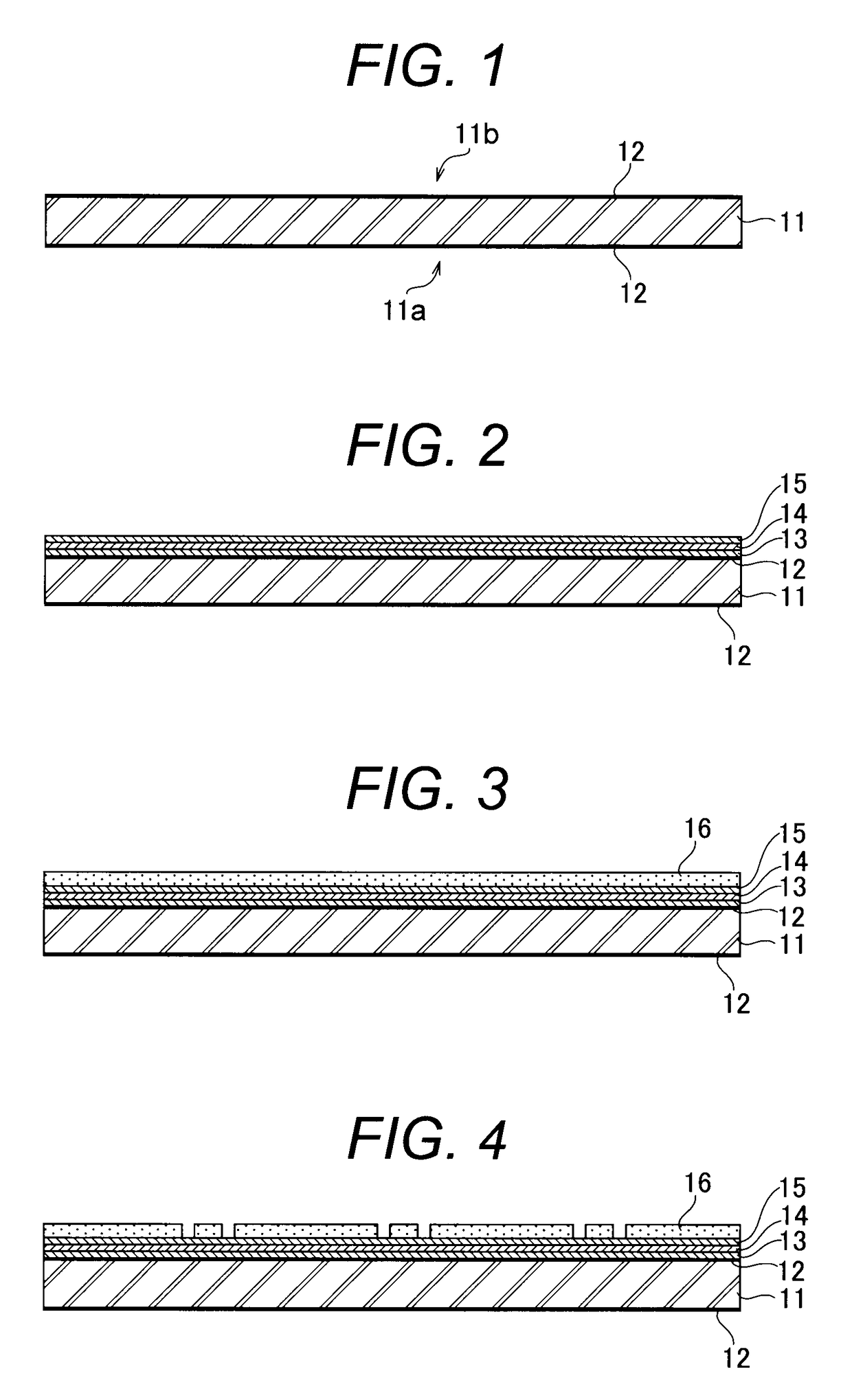
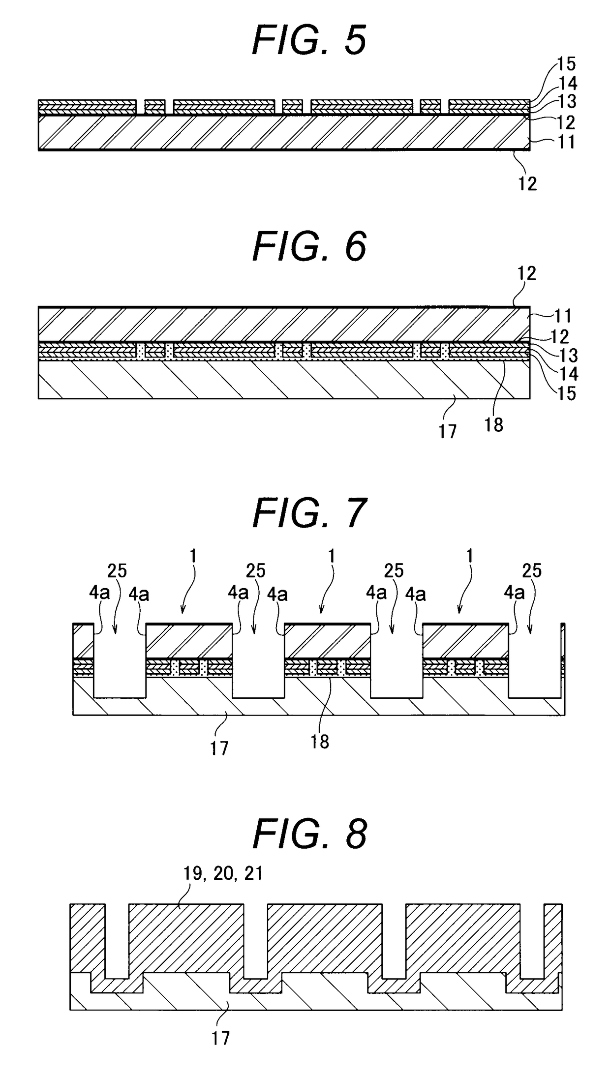
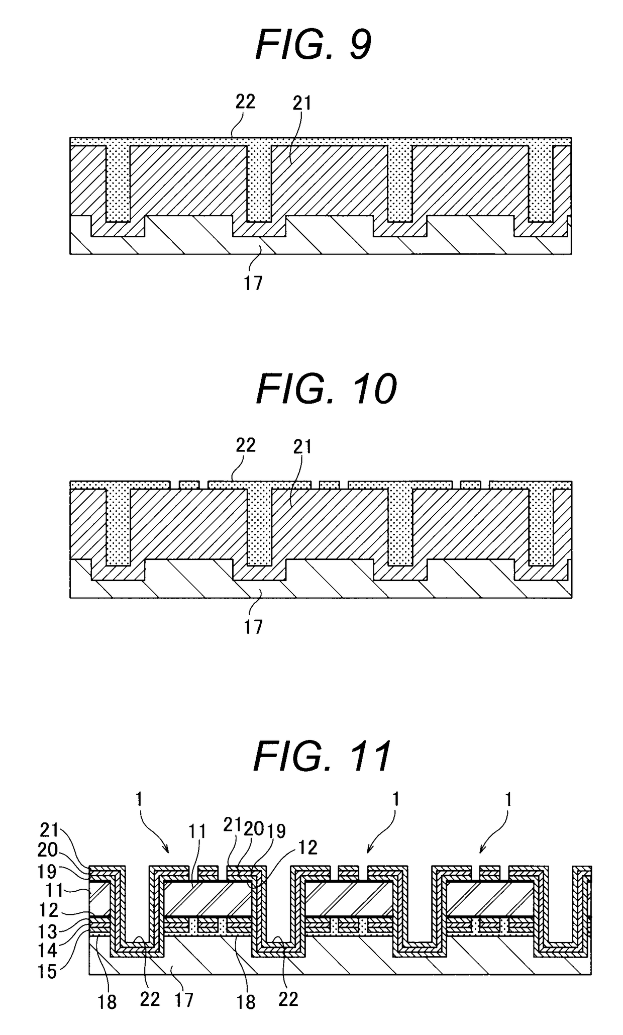
[0069]FIG. 1 to FIG. 13 sequentially shows the steps of a method for manufacturing an electronic component according to an embodiment of the present invention. The method for manufacturing an electronic component according to the embodiment is based on the premise of providing a chip component 1 having a rectangular parallelepiped (hexahedronal) overall shape as shown in FIG. 15, for example, with an aggregate of four terminal electrodes 5 corresponding to four peripheral surfaces 4a, 4a, 4b, and 4b so that each terminal electrode 5 has a U-shaped cross section (a U shape) that extends from a top surface 2 to the peripheral surface 4 (a side surface 4a or an end surface 4b) and to a bottom surface 3. As described previously, the number, the shape, and layout positions of the terminal electrodes 5 may apply various other aspects and it is therefore needless to say that the present invention will not be limited only to the illustrated example.

[0070]As shown in FIG. 1, a substrate 11 i...


PUM

PropertyMeasurementUnit
temperatureaaaaaaaaaa
thicknessaaaaaaaaaa

Abstract

A method for manufacturing an electronic component includes: a step of temporarily bonding a substrate to a support plate with an adhesive sheet; a step of forming a cut groove for dividing the substrate into individual chips by providing the substrate with a cut extending in the thickness direction from a second surface side, located opposite the first surface side, to a certain part of the support plate; a step of forming a continuous electrode on the second surface and on a peripheral surface located inside the cut groove, of each of the chips by sputtering, for example; and a step of detaching the chips from the support plate. An electrode on the first surface of the substrate may be formed prior to the temporary bonding step, and the electrode formed on the peripheral surface may be connected to the electrode on the first surface.

Description

BACKGROUND OF THE INVENTION[0001]The present invention relates to an electronic component and a method for manufacturing the same. More specifically, the present invention relates to a technique for forming a conductor such as a terminal electrode on an outer surface of a chip-shaped electronic component (hereinafter also simply referred to as a chip in some cases).[0002]Electronic components including various discrete components such as chip capacitors, chip inductors or chip resistors, and various electronic devices formed by combining multiple active and passive elements are offered today. Any of these electronic components needs terminal electrodes provided on the outer surface thereof so as to establish electrical and mechanical connection with the outside, thus being mounted on a wiring board.[0003]Such a terminal electrode has heretofore been formed, for instance, by: printing and coating a conductive material (a conductive paste or a conductive resin) at a predetermined posi...

Claims


Application Information

Patent Timeline
Patent Type & Authority Patents(United States)
IPC IPC(8): H05K3/02H01G4/252H01G4/30H01G13/00
CPCH01C1/148H01C17/281H01G4/232H01G4/248Y10T156/1052Y10T29/4979Y10T29/49156Y10T29/49128Y10T29/49163
Inventor KUWAJIMA, HAJIMEOHKUBO, HITOSHIOHTA, MANABU
Owner TDK CORPARATION
Why Eureka
Try Eureka