Circuit board and method of manufacturing same

a technology of circuit boards and solder terminals, applied in the field of circuit boards, can solve the problems of difficult to use organic circuit boards, and difficult to shorten the distance between the solder terminals, etc., to achieve a sufficient thickness of the solder pre-coat and shorten the connection distance

Inactive Publication Date: 2011-03-22
SHARP KK
View PDF10 Cites 1 Cited by
  • Summary
  • Abstract
  • Description
  • Claims
  • Application Information

AI Technical Summary

Benefits of technology

[0038]In view of the problems described above, an object of the technology described herein is to provide a circuit board and a method of manufacturing the circuit board, the circuit board and method allowing a further shorter connection distance between electrodes of a semiconductor device, and also allowing a sufficient thickness of a solder pre-coat in a soldering process.
[0042]Therefore, it is possible to take a wide distance between each of the bonding pads. In short, each of the bonding pads is so positioned that the bonding pads are hardly short-circuited electrically. That is to say, the technology described herein can provide a circuit board, with which it is possible to form connecting portions with high density, the connecting portions including a plurality of the bonding pads positioned adjacently, and a method of manufacturing the circuit board.

Problems solved by technology

However, the wire bonding method requires a circuit board to have a region for wire bonding, outside of the region where the semiconductor chip is mounted.
Therefore, a package size is not compact.
However, these methods have problems as follows.
In the reflow process, it is difficult to use an organic circuit board because the semiconductor chip and the circuit board are heated.
In addition, it is also difficult to shorten (fine-pitch) the distance between the solder terminals, because the solder bumps should be formed.
As an unfortunate result, the whole process gets complicated.
The ACF method has a problem as well.
However, the decrease in the amount of the solder for pre-coating reduces an amount of solder contributing to the connection of the bonding pad 730 with a gold wire bump, formed on an electrode pad of a semiconductor chip, thereby resulting in a problem of unstable connections between the gold wire bump and the bonding pad 730.
However, with bonding pads fine-pitched and being long and thin, as FIG. 11(b) shows, molten solder gathers at random positions because of surface tension caused in soldering the semiconductor chip and the bonding pads together.
Therefore, a possibility of bonding gold wire bumps of a semiconductor chip and molten solder together successfully decreases, thereby causing bad connections.
However, with the conventional arrangements described above, it is difficult to make a circuit board, with which it is possible to narrow the connection distance between the electrodes of a semiconductor device, and also to have a sufficient thickness of the solder pre-coat for the soldering process at the same time.
In short, connection defects would occur because the amount of solder for connecting a gold wire bump to a bonding pad is not sufficient.

Method used


Image

  • Circuit board and method of manufacturing same
  • Circuit board and method of manufacturing same
  • Circuit board and method of manufacturing same

Examples


Embodiment Construction

[0072]One example embodiment of the technology described herein is described below referring to FIGS. 1(a) to 7(b).

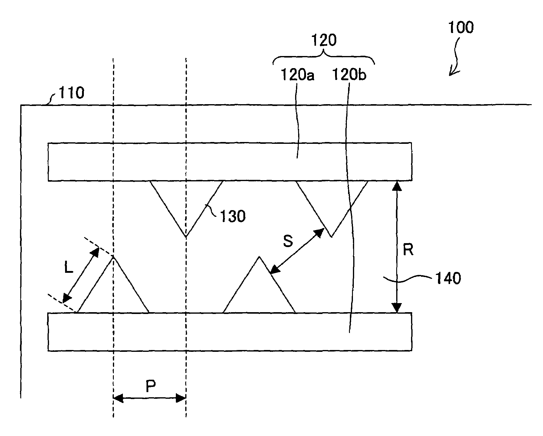
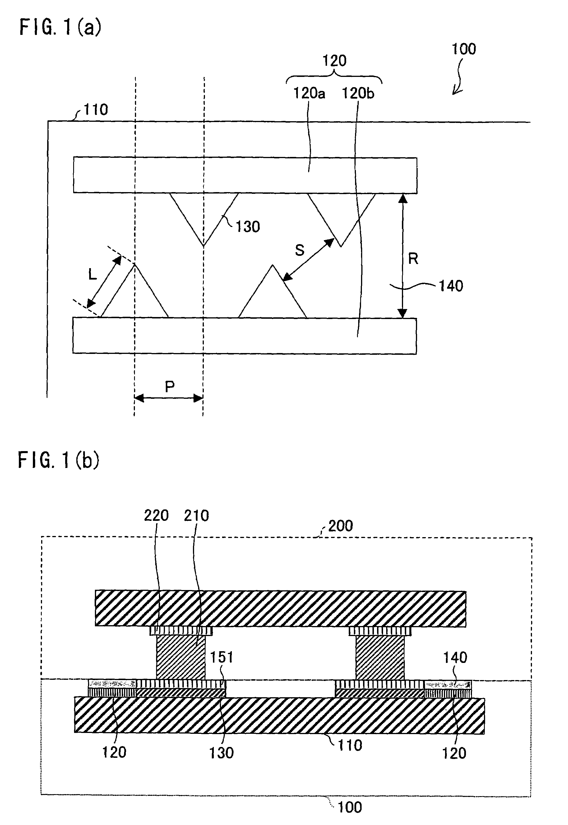
[0073]FIG. 1(a) is a plan view of a flip-chip board 100 in accordance with an example embodiment of the technology described herein, and FIG. 1(b) is a cross-section view showing a case where the flip-chip board 100 and a semiconductor chip 200 in accordance with the example embodiment of the technology described herein are bonded together by flip-chip bonding.

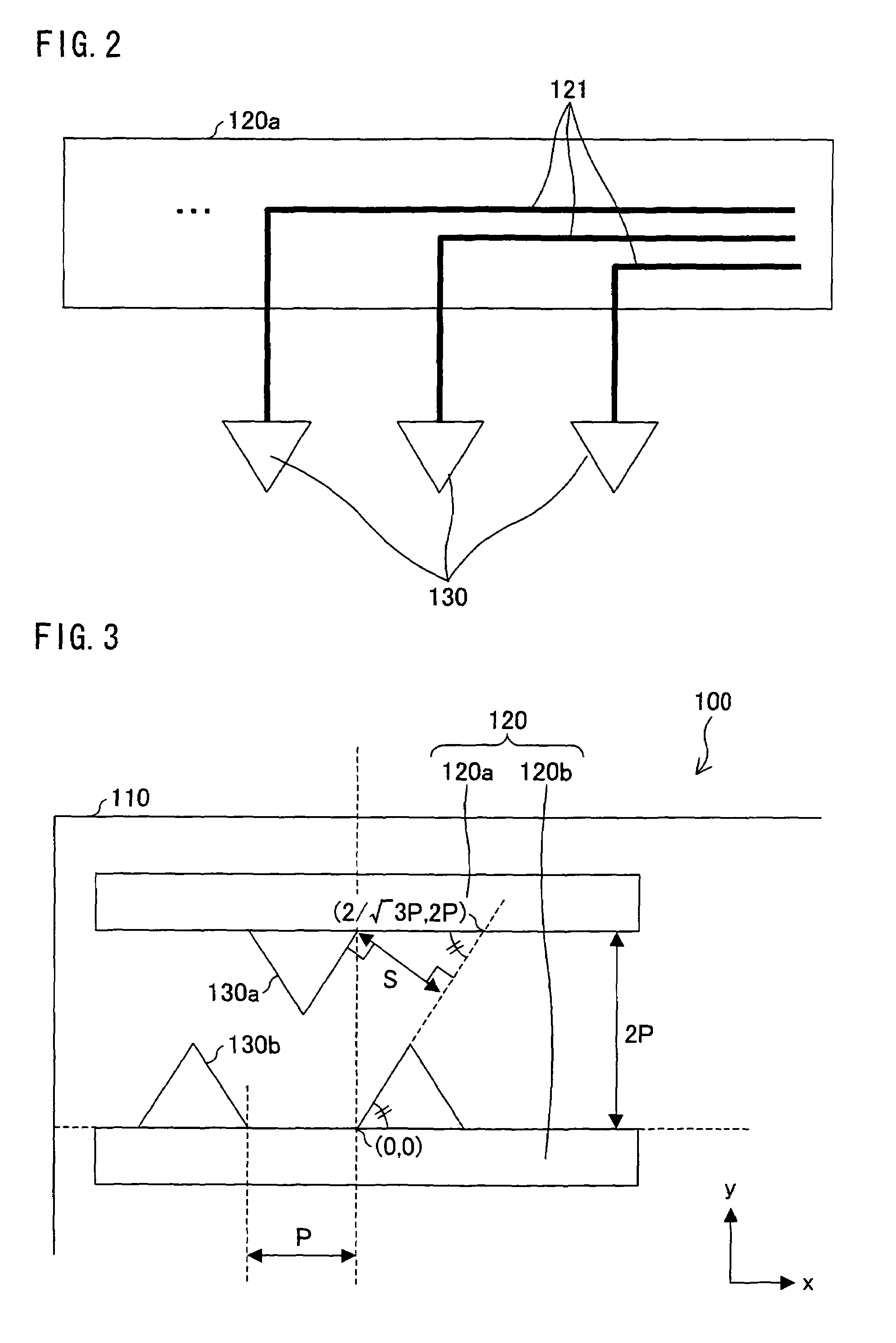
[0074]The flip-chip board (circuit board) 100 in accordance with the example embodiment of the technology described herein includes a circuit pattern (not shown in FIGS. 1(a) and 1(b)) provided on a surface of a board 110, and a plurality of conductor patterns 120 (which are lead wires; FIG. 1(a) shows two conductor patterns, 120a and 120b) electrically connected to the circuit pattern. On each of the conductor patterns 120, a bonding pad 130 is provided. The bonding pad 130 electrically connects a bump 210 of a s...


PUM

PropertyMeasurementUnit
distanceaaaaaaaaaa
lengthaaaaaaaaaa
widthaaaaaaaaaa

Abstract

The present invention provides a circuit board and a method for manufacturing the circuit board, the circuit board and method allowing a further shorter connection distance between electrodes of a semiconductor device, and also allowing a sufficient thickness of a solder pre-coat in a soldering process. The circuit board comprises bonding pads for being connected with bumps of a semiconductor element, which act as connection terminals, the bonding pads being arrayed in parallel lines on a surface of the circuit board, and, on the adjacent parallel lines, the bonding pads being positioned to form a zigzag pattern along the parallel lines longitudinally.

Description

[0001]This Nonprovisional application claims priority under 35 U.S.C. §119(a) on Patent Application No. 094984 / 2007 filed in Japan on Mar. 30, 2007, the entire contents of which are hereby incorporated by reference.FIELD OF THE INVENTION[0002]The present invention relates to a circuit board and a method of manufacturing the same, in particular, to a shape of electrodes formed on a board on which a flip-chip is to be mounted.BACKGROUND OF THE INVENTION[0003]With semiconductor devices becoming lighter, thinner and smaller, necessary components of devices have been miniaturized significantly.[0004]Conventionally, a wire bonding method is used for electrical connections between a semiconductor chip and a circuit board. Japanese Unexamined Patent Application Publication No. 11-121526 (published on Apr. 30, 1999) (Patent Document 1) discloses a technique, with which, to electrode pads formed on a miniaturized semiconductor chip, gold wires are wire-bonded at bonding positions shifted alte...

Claims


Application Information

Patent Timeline
Patent Type & Authority Patents(United States)
IPC IPC(8): H05K7/00
CPCH01L23/49816H01L23/49838H05K1/111H01R12/714H01L2224/16H01L2924/01078H01L2924/01079Y10T29/49204H05K3/3484H05K2201/09381H05K2201/09709H05K2201/10674H05K2203/043H05K3/3436H01L2224/0554H01L2224/05568H01L2224/05573H01L2224/05624H01L2224/05647H01L2224/16238H01L2924/00014H05K3/3485Y02P70/50H01L2224/05599H01L2224/0555H01L2224/0556
Inventor ONO, ATSUSHI
Owner SHARP KK
Why Eureka
Try Eureka