Switch circuit for high frequency signals wherein distortion of the signals are suppressed

a high-frequency signal and switch circuit technology, applied in electronic switching, pulse technique, semiconductor devices, etc., can solve the problems of high-frequency signal having passed through the high-frequency switch circuit entail distortion, high-frequency signal distortion, etc., to reduce distortion and reduce the distortion of high-frequency signals.

Active Publication Date: 2011-03-29
NEC CORP
View PDF17 Cites 8 Cited by
  • Summary
  • Abstract
  • Description
  • Claims
  • Application Information

AI Technical Summary

Benefits of technology

It is therefore an object of the present invention to provide a high-frequency switch circuit capable of reducing distortion that arises when a high-frequency signal passes through it.
In the high-frequency switch circuit constructed as above, application of a voltage lower than the voltage of the control signal to the passage route of the high-frequency signal causes the potential at the RF node to become lower and the voltage applied to the gate terminal of the field effect transistor to become higher. As a result, the on-state resistance in the field effect transistor being in the on-state becomes lower, so that the variation of the on-state resistance of the field effect transistor relative to the variation in the voltage of the high-frequency signal input from the drain terminal or source terminal is suppressed. On the other hand, since the input resistance of the field effect transistor being in the off-state is high, the bias voltage is applied as it is to the drain terminal and source terminal so that it is possible to impart a potential difference between the drain and source terminals. As a result, the variation in the off-state capacitance of the field effect transistor relative to the voltage variation of the high-frequency signal input from the drain terminal or source terminal can be suppressed. Accordingly, it is possible to reduce distortion of the high-frequency signal that arises when the signal passes through the high-frequency switch circuit.

Problems solved by technology

In this high-frequency switch circuit of the prior art shown in FIG. 1, as described in paragraph 0009 in Japanese Patent Application Laid-open 2004-320439, for example, the value of the resistance between the drain and source of each FET that is in the off-state (off-state resistance) is extremely large, hence there is the problem that the potential between the drain and source terminals of each of the serially connected FETs becomes unstable.
In the high-frequency switch circuits using FETs as above, there is a problem in which the high-frequency signal having passed through the high-frequency switch circuit entails distortion.
This phenomenon in which the FET on-state resistance and off-state capacitance vary depending on the input voltage causes distortion of the high-frequency signal that has passed through the high-frequency switch circuit.

Method used


Image

  • Switch circuit for high frequency signals wherein distortion of the signals are suppressed
  • Switch circuit for high frequency signals wherein distortion of the signals are suppressed
  • Switch circuit for high frequency signals wherein distortion of the signals are suppressed

Examples


first exemplary embodiment

The First Exemplary Embodiment

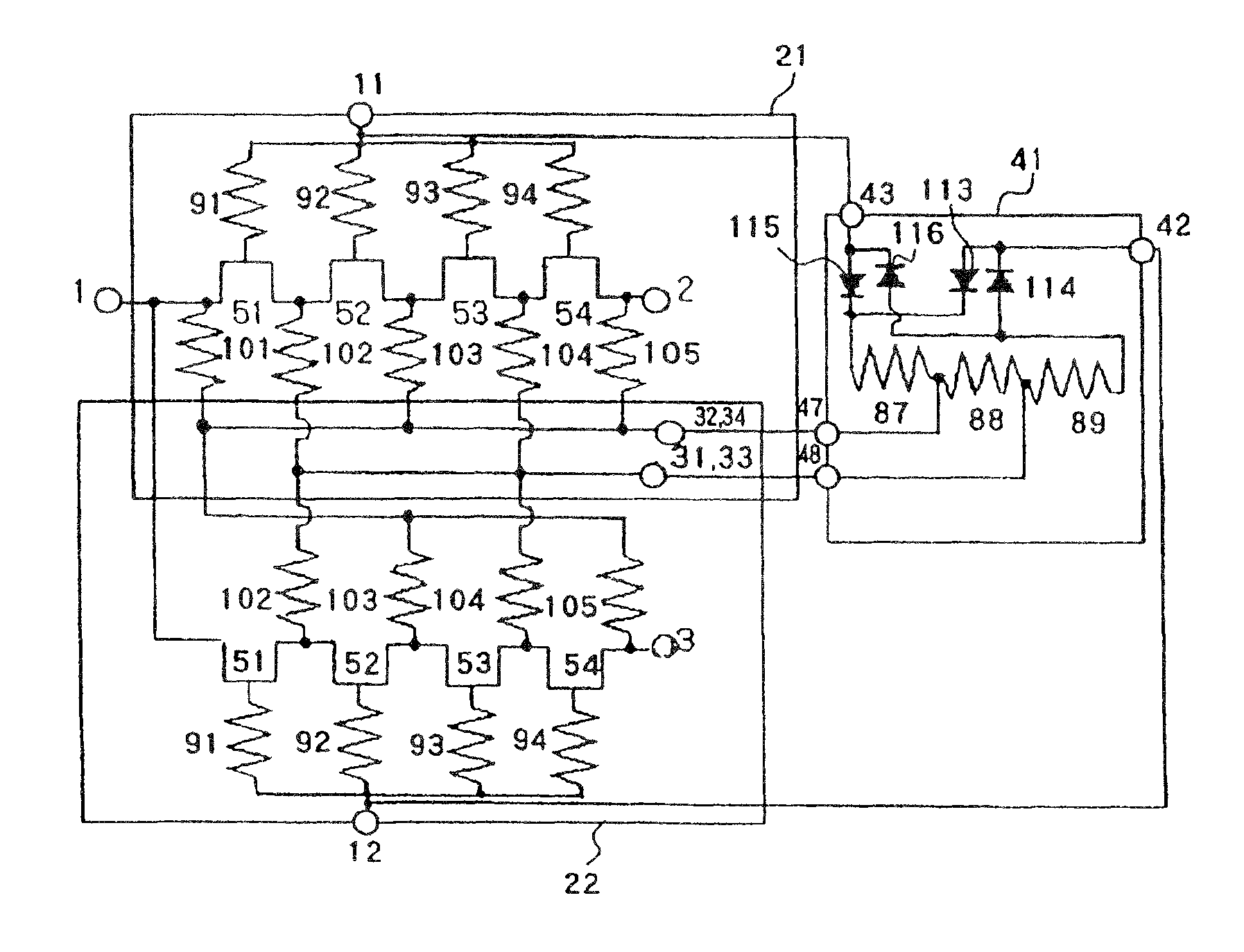
FIG. 4 is a block diagram showing a configuration of a high-frequency switch circuit of the first exemplary embodiment. Here, FIG. 4 is an example in which the configuration of the first exemplary embodiment is applied to a SPDT type high-frequency switch circuit.

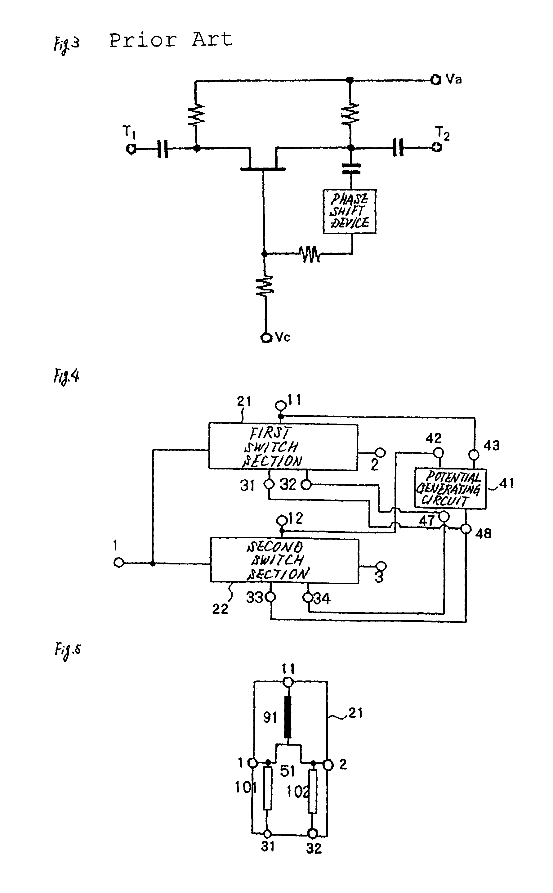
As shown in FIG. 4, the high-frequency switch circuit of the first exemplary embodiment has a configuration including: first switch section 21 and second switch section 22 for allowing a high-frequency signal to pass or for cutting off a high-frequency signal; and a potential generating circuit 41 for supplying predetermined bias voltages to first switch section 21 and second switch section 22.

First switch section 21 is interposed between first high-frequency terminal 1 and second high-frequency terminal 2 for input and output of a high-frequency signal, and second switch section 22 is interposed between first high-frequency terminal 1 and third high-frequency terminal 3 for input and output of...

second exemplary embodiment

The Second Exemplary Embodiment

FIG. 25 is a block diagram showing a configuration of a high-frequency switch circuit of the second exemplary embodiment. Here, FIG. 25 is an example in which the configuration of the second exemplary embodiment is applied to a DPDT (double pole double through) type high-frequency switch circuit.

As shown in FIG. 25, the high-frequency switch circuit of the second exemplary embodiment includes: first switch section 21, second switch section 22, third switch section 23 and fourth switch section 24 for allowing a high-frequency signal to pass through or for cutting off a high-frequency signal; and a potential generating circuit 41 for supplying predetermined bias voltages to first switch section 21 through fourth switch section 24.

First switch section 21 is interposed between first high-frequency terminal 1 and second high-frequency terminal 2 for input and output of a high-frequency signal, and second switch section 22 is interposed between second high-f...


PUM


Abstract

A high-frequency switch circuit includes: a switch section comprised of a field effect transistor having a plurality of bias circuits and a potential generating circuit for generating bias voltages from a control signal and supplying them to the bias circuits. The field effect transistor forms the passage route of a high-frequency signal by turning on and off in accordance with the control signal. The bias circuits are provided to produce a potential difference between the drain terminal and the source terminal of the field effect transistor and to apply bias voltages lower than the voltage of the control signal to the drain terminal, and the source terminal.

Description

TECHNICAL FIELDThis application is based upon and claims the benefit of priority from Japanese patent application No. 2006-142575, filed on May 23, 2006, the disclosure of which is incorporated herein in its entirety by reference.The present invention relates to a high-frequency switch circuit for passing or cutting off a high-frequency signal.BACKGROUND ARTAs a high-frequency switch circuit for passing or cutting off a high-frequency signal or for allowing a high-frequency signal to pass through, those using diodes and those using field effect transistors (FET: field effect transistor) have been conventionally known.FIG. 1 is an example of a high-frequency switch circuit using FETs, a circuit diagram showing a high-frequency switch circuit configuration of a SPDT (single pole double through) type. Here, FIG. 1 is a circuit disposed in FIG. 1 of Japanese Patent Application Laid-open H08-139014.The high-frequency switch circuit shown in FIG. 1 has a configuration including first swit...

Claims


Application Information

Patent Timeline
Patent Type & Authority Patents(United States)
IPC IPC(8): H03K17/60
CPCH03K17/165H03K17/693
Inventor TAKAHASHI, YUJINUMATA, KEIICHI
Owner NEC CORP
Why Eureka
Try Eureka