

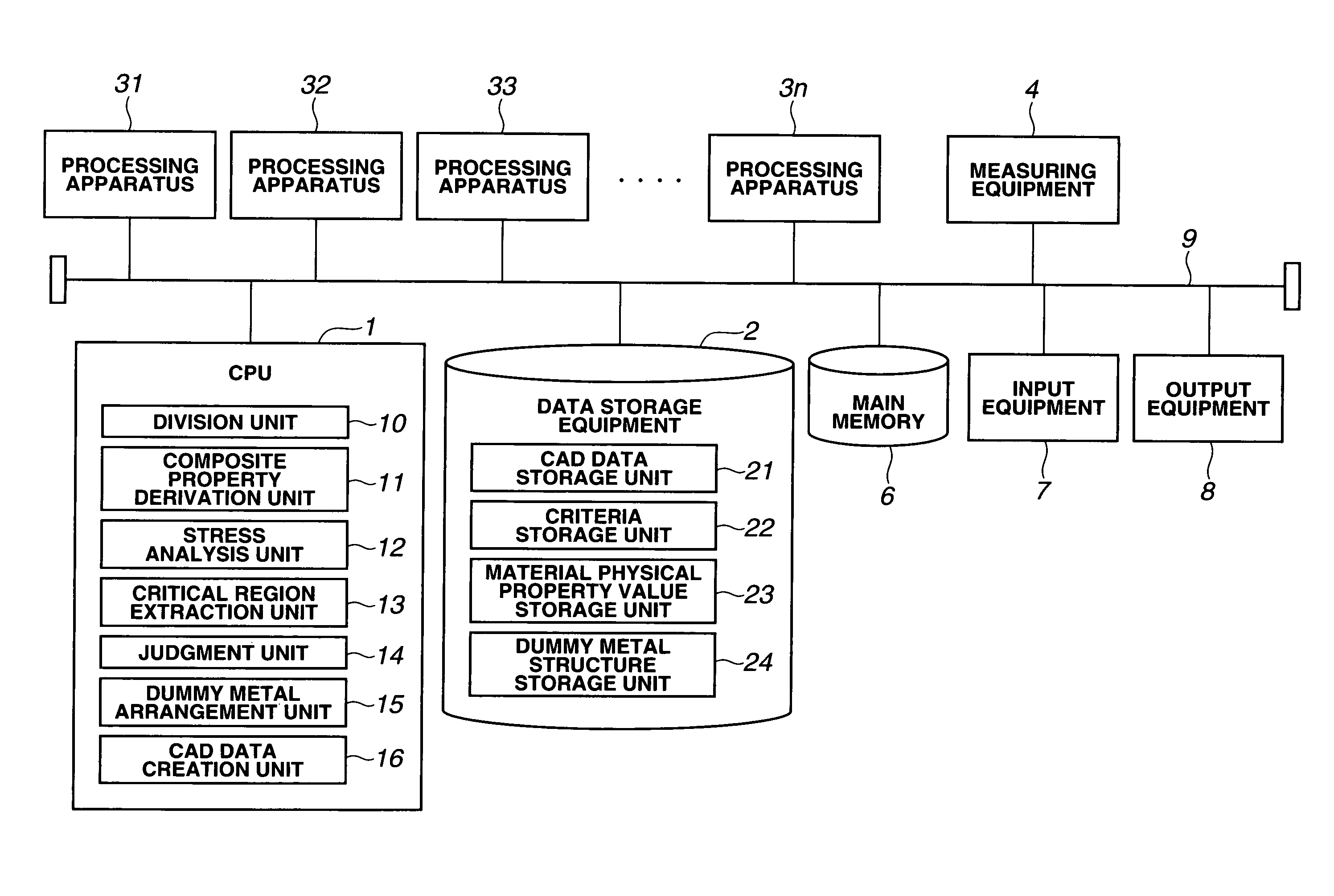
Stress analysis method, wiring structure design method, program, and semiconductor device production method
a stress analysis and stress analysis technology, applied in the direction of pressure difference measurement between multiple valves, instruments, digital computer details, etc., can solve the problems of low dielectric constant film mechanical strength deterioration, low dielectric constant film strength in its material itself, and deterioration of adhesion strength in the interface of stacked film including low dielectric constant film
- Summary
- Abstract
- Description
- Claims
- Application Information
AI Technical Summary
Benefits of technology
Problems solved by technology
Method used
Image

Examples
first modified example
[0094]In a first modified example of the embodiment of the present invention, fracture criteria measurement for a defect that a crack arises in an insulating film under a pad at the time of normal stress application to the pad in a probing process, a bonding process, etc. will be explained as another example of fracture criteria measurement. Although this defect is a defect that a crack arises in an SiO2 film under a top layer pad in a semiconductor device which has a multi-layer structure using a low dielectric constant film as an inter-layer insulating film, it is not necessary to produce a sample with a multi-layer structure at the time of fracture criteria measurement. What is necessary is just to produce a sample which has at least one layer of wiring layer and an SiO2 film for fracture criteria measurement as its upper layer. It is sufficient to produce an AL pad on an SiO2 film, or it may be possible to perform the fracture criteria measurement without producing the AL pad de...
second modified example
[0104]As a second modified example of the embodiment of the present invention, optimization of dummy metals for defects related to multilayering will be explained. Even with a structure, where a defect is not observed in a single-layer structure, a defect may be observed in a via connecting portion etc. by multilayering it. In order to suppress defect occurrence at the time of adding a heat load from room temperature to 450° C., dummy metal arrangement is optimized.
[0105]The second modified example of the embodiment of the present invention, as shown in FIG. 12, is intended for a chip with a multi-layer structure which has wiring layers M1 and M2, and a via layer V2 connecting the wiring layers M1 and M2, and has a desired wiring structure. Thus, an inter-layer insulating film 143a in which the wiring layer M1 is embedded and is formed, an etching stop film 143b, an inter-layer insulating film 143c in which the via layer V2 is embedded and is formed, and an inter-layer insulating fi...
third modified example
[0111]As a third modified example of the embodiment of the present invention, an optimization method of dummy metals to defects in the case of applying an external load will be explained. In order to suppress an insulating film breakdown arising under a pad when an external load is applied to the pad at the time of probing, dummy metal arrangement is optimized.
[0112]As shown in FIG. 13, the third modified example of the embodiment of the present invention is intended for a chip which has desired wiring structures of wiring layers M1 to M6 respectively, and which further has an AL pad layer which includes AL pads 151 and 152 as an upper layer of the wiring layer M6. A plane size of the chip is 22 mm×19 mm.
[0113]The division unit 10 shown in FIG. 1 divides the 22 mm×19 mm chip into 200 μm×200 μm square regions (analysis areas) per each of the wiring layers M1 to M6 and per the AL pad layer. The composite property derivation unit 11 extracts wiring structure data on the wiring layers M...
PUM
 Abstract
Description
Claims
Application Information