Method for forming thin film and film-forming device

a film-forming device and film-forming technology, applied in the direction of superimposed coating process, liquid/solution decomposition chemical coating, manufacturing tools, etc., can solve the problems of loss of uniform film thickness of the substrate surface, disadvantageous influence of later processes, various problems, etc., to prevent the fluidity of the coating solution during the treatment of forming the film, the effect of facilitating the treatment of the substra

Inactive Publication Date: 2011-04-19
TOKYO ELECTRON LTD
View PDF14 Cites 2 Cited by
  • Summary
  • Abstract
  • Description
  • Claims
  • Application Information

AI Technical Summary

Benefits of technology

[0010]Preferably, the method for forming a thin film according to the present invention further includes the step of stabilizing the film properties of the thin film by heating the substrate after the formation of the thin film on the surface of the substrate.
[0013]According to the present invention, the following effects can be achieved.
[0015]In addition, in the present invention, charged particles of the coating solution are electrostatically adhered to the substrate charged with an electrical potential opposite to the charge of the particles by electrical attraction. Therefore, the adhered state of the particles lasts for a long time, and later treatment of the substrate can be readily performed. Furthermore, in the present invention, the spraying of the coating solution is conducted in a treatment chamber which is isolated from the air and is maintained with a solvent gas atmosphere. Therefore, drying of the coating solution is avoided, and the fluidity of the sprayed coating solution is prevented. Additionally, directions that the charged particles are electrostatically moved are not influenced by the air.
[0016](2) Exhaustion of the solvent gas from the treatment chamber is not conducted during the formation of a thin film but is conducted after the formation of the thin film. Therefore, the fluidity of the coating solution during the treatment for forming the film can be prevented and, thereby, uniformity in the thickness of the thin film is further achieved, in addition to the effects described in the above (1).
[0017](3) Since the substrate is heated after the formation of a thin film, the film properties of the thin film can be stabilized. Therefore, the thin film can be surely formed, in addition to the effects described in the above (1) and (2).

Problems solved by technology

Therefore, uniformity in the film thickness of the substrate surface is lost.
If nonuniformity occurs in the film thickness, later processes are disadvantageously influenced.
Thus, various problems arise.

Method used


Image

  • Method for forming thin film and film-forming device
  • Method for forming thin film and film-forming device
  • Method for forming thin film and film-forming device

Examples


Embodiment Construction

[0024]The preferred embodiments of the present invention will now be described with reference to the appended drawings.

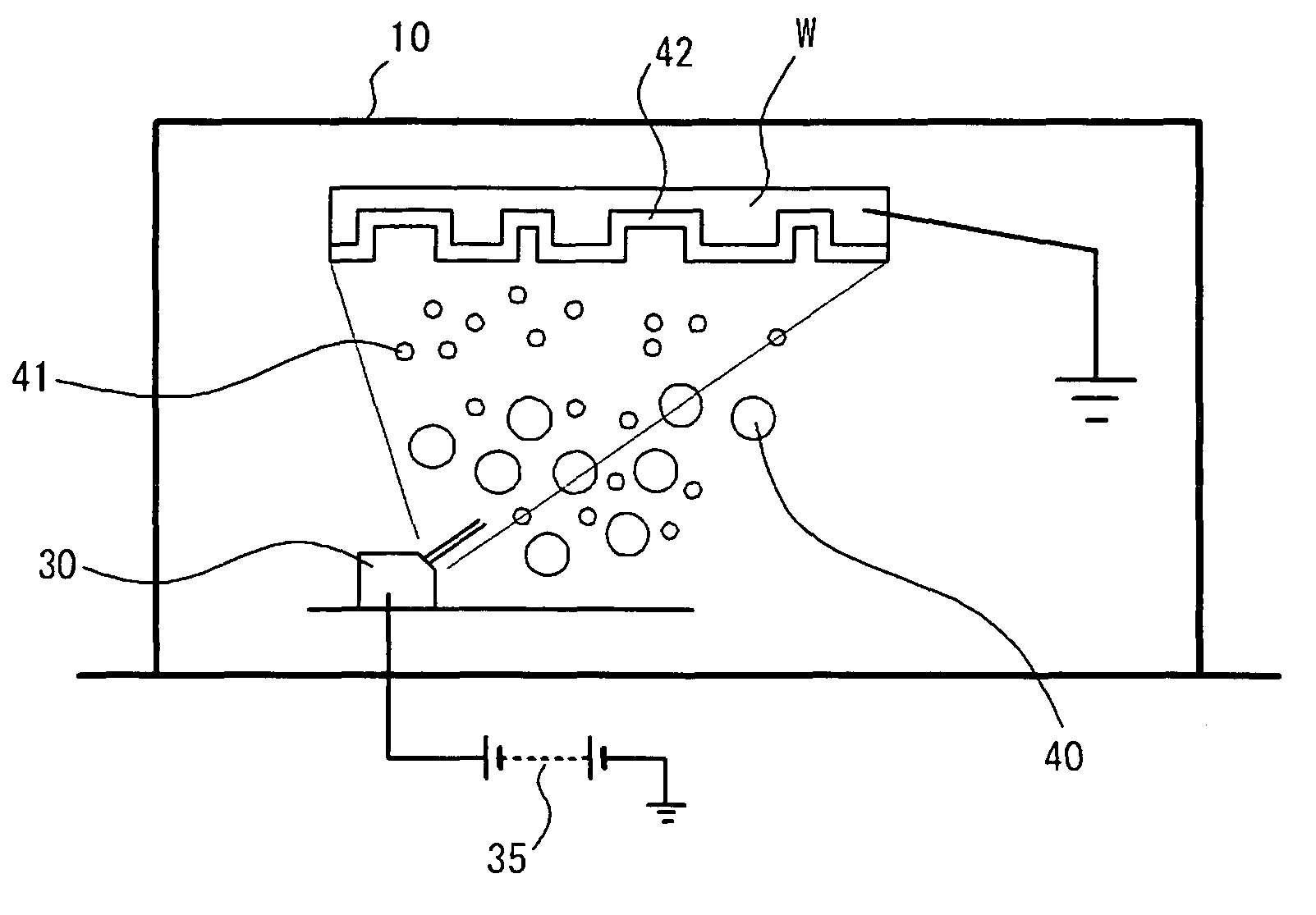
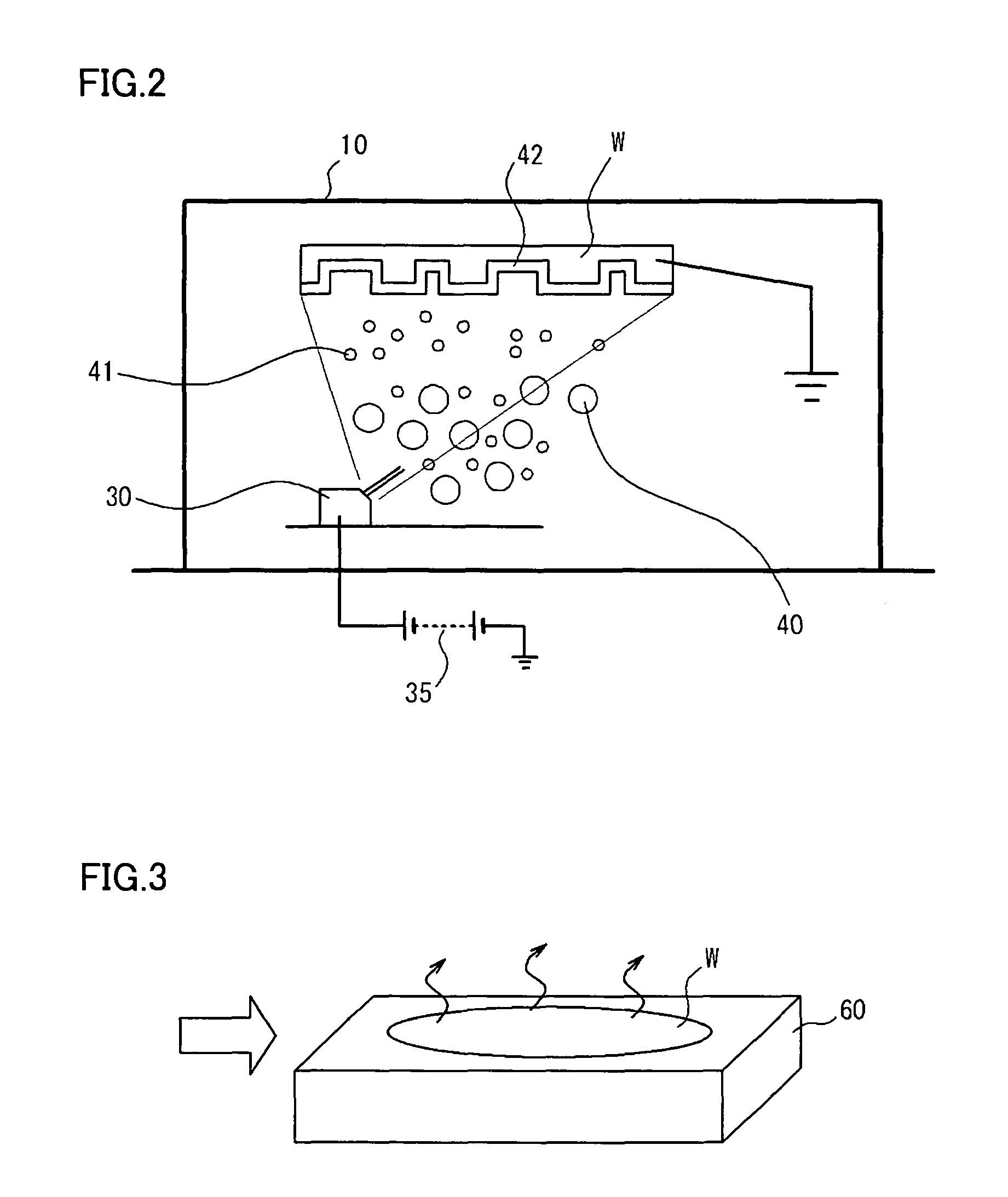
[0025]FIG. 1 is a resist-coating device as an example of the film-forming device for forming a thin film according to an embodiment of the present invention.

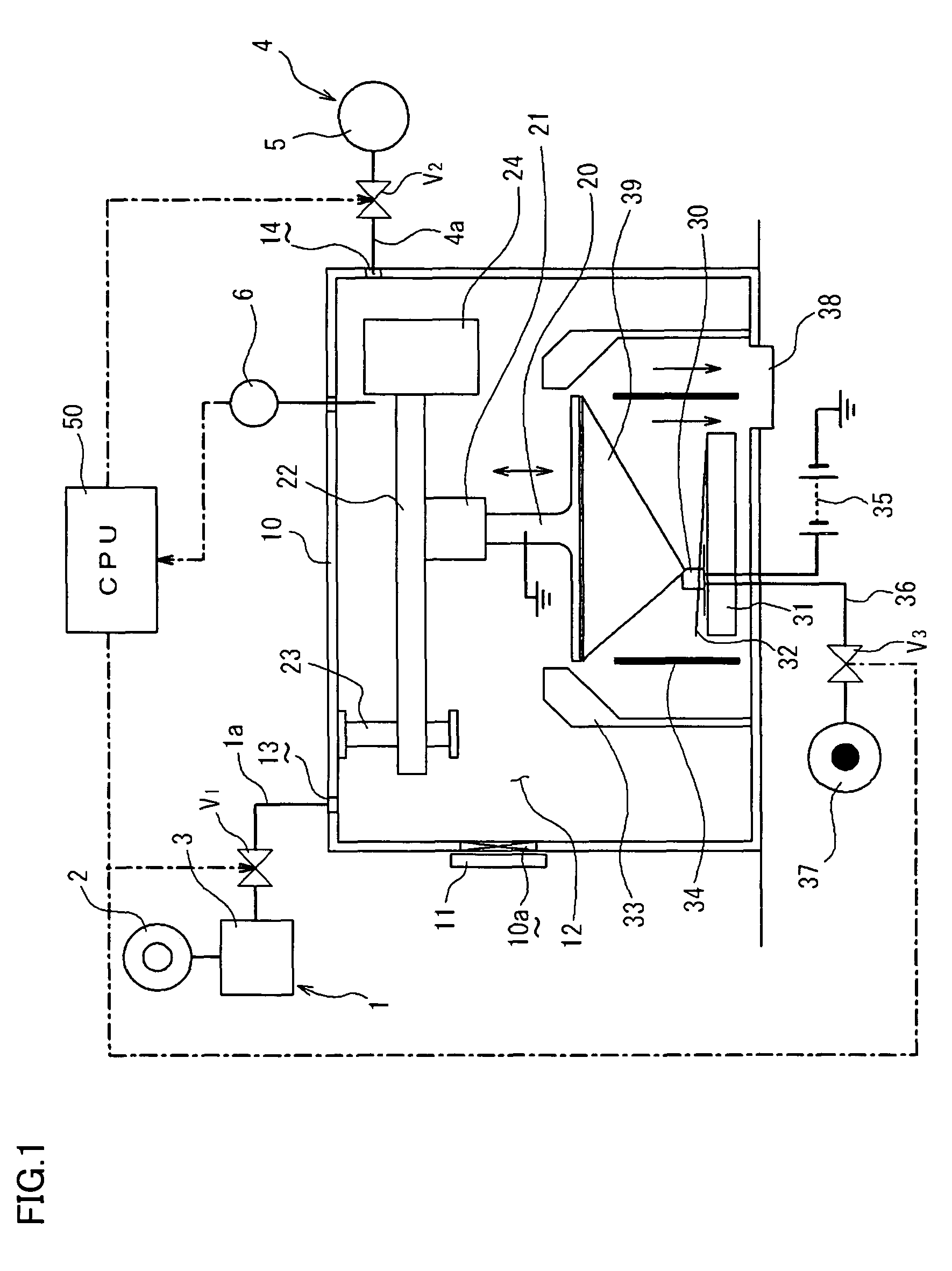
[0026]As shown in FIG. 1, the resist-coating device includes a housing 10 to form a treatment chamber 12 which can be isolated from the air. The housing 10 is provided with an opening 10a for taking a wafer W in and out. The opening 10a is opened and closed by a shutter 11 which is driven by a lifting and lowering portion (not shown) so as to move up and down. The inside of the housing 10 is provided with a chuck 20 serving as a holding portion for holding a semiconductor wafer W (hereinafter referred to as a wafer W) as a substrate to be processed, a motor 21 serving as a rotating portion for rotating the chuck 20, and a supporting member 22 for supporting the chuck 20 and the motor 21 at the upper side thereof...


PUM

PropertyMeasurementUnit
temperatureaaaaaaaaaa
electrical potentialaaaaaaaaaa
relative distanceaaaaaaaaaa

Abstract

It is an object to provide a method for forming a thin film having a uniform thickness so as to follow asperities of a surface of a wafer to be processed and to provide a film-forming device used for the method. The film-forming device includes a treatment chamber for receiving a wafer and isolating the wafer from the air; a solvent-gas-supplying portion for supplying a solvent gas into the treatment chamber; a chuck for rotatably holding the wafer so that the downward-facing surface of the substrate is the surface on which a thin film is formed; a coating-solution-supplying portion for supplying a coating solution as a mist of charged particles toward the surface of the wafer; and a charging portion for charging the wafer with an electrical potential opposite to the charge of the particles.

Description

BACKGROUND OF THE INVENTION[0001]1. Field of the Invention[0002]The present invention relates to a method for uniformly forming a thin film on a substrate surface having asperities thereon and further relates to a device used for the method.[0003]2. Description of the Background Art[0004]In general, in manufacturing processes of semiconductor wafers, photolithography technology is used for forming resist patterns on surfaces of substrates (substrates to be processed) such as semiconductor wafers or LCD substrates. This photolithography technology includes a resist-applying step for applying a resist solution to a surface of a substrate to be processed, an exposure treatment step for exposing the resulting resist film to a circuit pattern, and a development treatment step for supplying a developing solution to the substrate after the exposure treatment step. In such a case, the resist-applying step employs a so-called spin-coating method, namely, placing a substrate on a rotatable mo...

Claims


Application Information

Patent Timeline
Patent Type & Authority Patents(United States)
IPC IPC(8): B05B5/025B05C11/02
CPCH01L21/6715
Inventor TERADA, SHOUICHIMIZUNO, TSUYOSHIUEHARA, TAKESHI
Owner TOKYO ELECTRON LTD
Why Eureka
Try Eureka